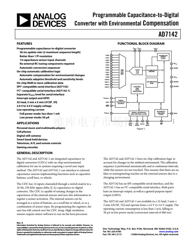
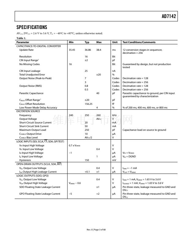
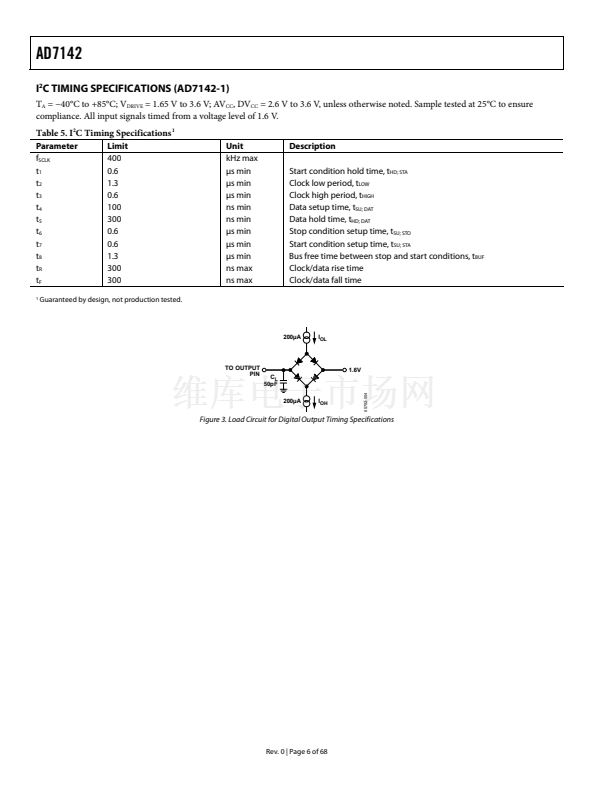
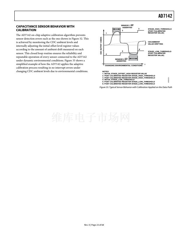
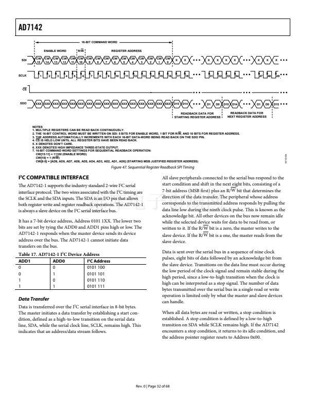
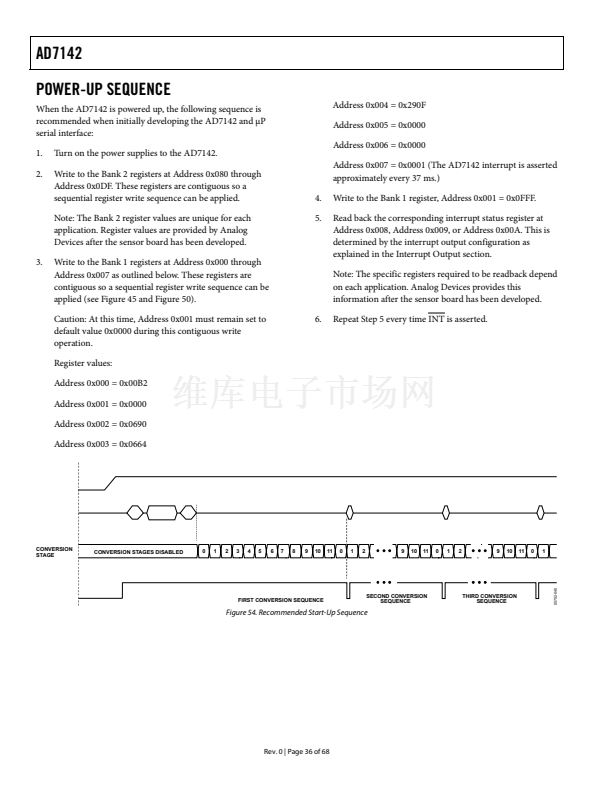
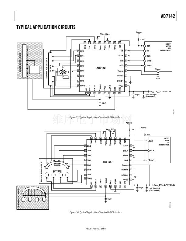
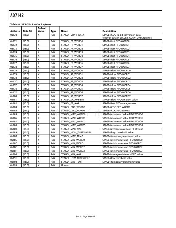
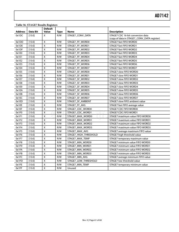
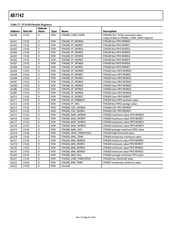
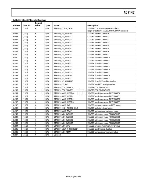
AD7142
SERIAL INTERFACE
The AD7142 is available with an SPI serial interface. The
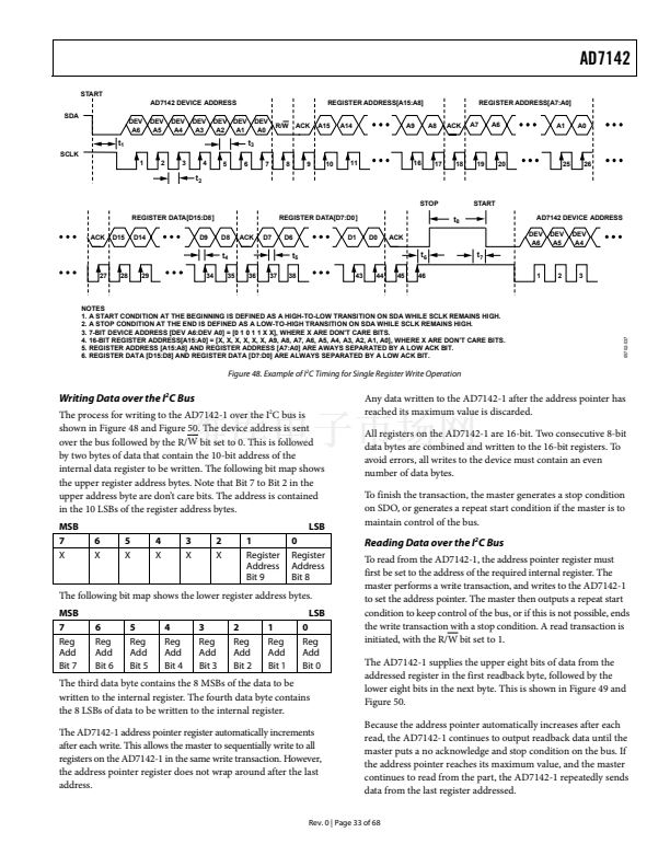
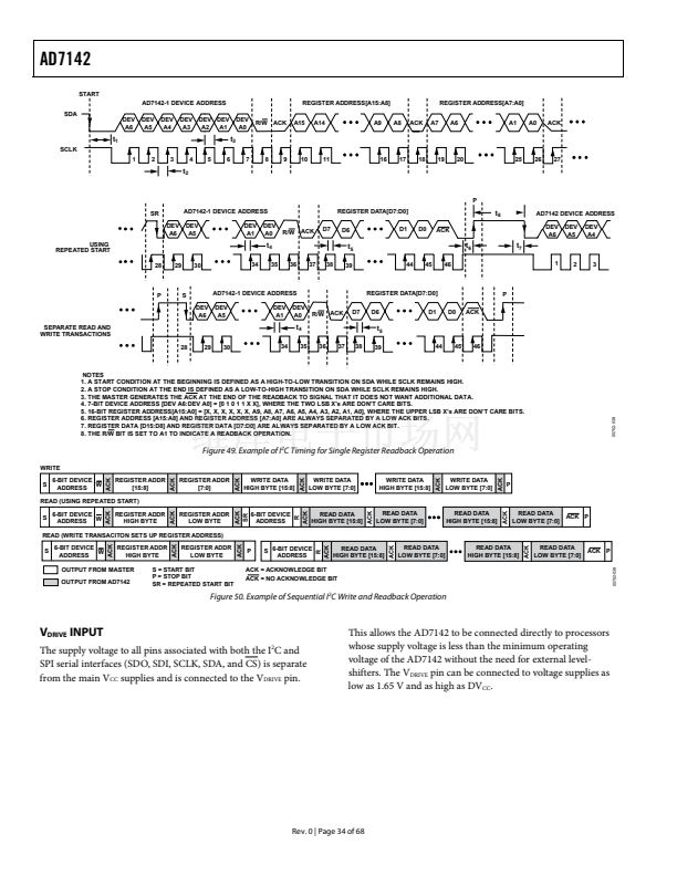
AD7142-1 is available with an I
2
C-compatible interface. Both
parts are the same, with the exception of the serial interface.
Bits[15:11] of the command word must be set to 11100 to
successfully begin a bus transaction.
Bit 10 is the read/write bit; 1 indicates a read, and 0 indicates a
write.
Bits[9:0] contain the target register address. When reading or
writing to more than one register, this address indicates the
address of the first register to be written to or read from.
SPI INTERFACE
The AD7142 has a 4-wire serial peripheral interface (SPI). The
SPI has a data input pin (SDI) for inputting data to the device, a
data output pin (SDO) for reading data back from the device,
and a data clock pin (SCLK) for clocking data into and out of
the device. A chip select pin (CS) enables or disables the serial
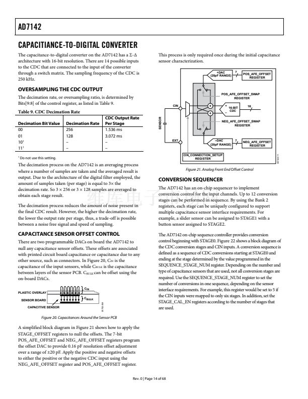
interface. CS is required for correct operation of the SPI
interface. Data is clocked out of the AD7142 on the negative
edge of SCLK, and data is clocked into the device on the
positive edge of SCLK.
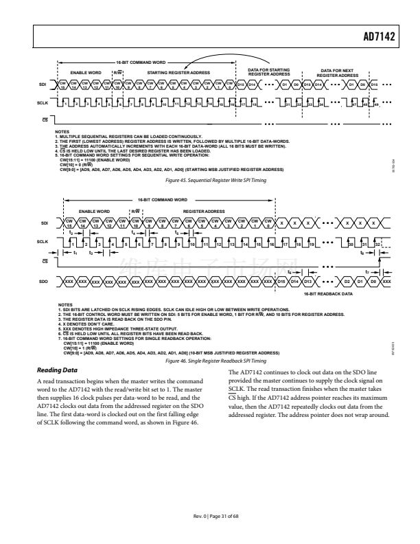
Writing Data
Data is written to the AD7142 in 16-bit words. The first word
written to the device is the command word, with the read/write
bit set to 0. The master then supplies the 16-bit input data-word
on the SDI line. The AD7142 clocks the data into the register
addressed in the command word. If there is more than one
word of data to be clocked in, the AD7142 automatically incre-
ments the address pointer, and clocks the next data-word into
the next register.
The AD7142 continues to clock in data on the SDI line until
either the master finishes the write transition by pulling CS
high, or until the address pointer reaches its maximum value.
The AD7142 address pointer does not wrap around. When it
reaches its maximum value, any data provided by the master on
the SDI line is ignored by the AD7142.
SPI Command Word
All data transactions on the SPI bus begin with the master
taking CS from high to low and sending out the command
word. This indicates to the AD7142 whether the transaction is a
read or a write, and gives the address of the register from which
to begin the data transfer. The following bit map shows the SPI
command word.
MSB
15
14
1
1
LSB
13
1
12
0
11
0
10
R/W
9:0
Register address
16-BIT COMMAND WORD
ENABLE WORD
SDI
CW
15
CW
14
CW
13
CW
12
CW
11
R/W
CW
10
CW
9
CW
8
CW
7
REGISTER ADDRESS
CW
6
CW
5
CW
4
CW
3
CW
2
CW
1
CW
0
D15
D14
D13
16-BIT DATA
D2
D1
D0
t
2
SCLK
1
2
t
3
3
4
5
t
4
6
7
8
t
5
9
10
11
12
13
14
15
16
17
18
19
30
31
32
t
1
CS
t
8
Figure 44. Single Register Write SPI Timing
Rev. 0 | Page 30 of 68
05702-033
NOTES
1. SDI BITS ARE LATCHED ON SCLK RISING EDGES. SCLK CAN IDLE HIGH OR LOW BETWEEN WRITE OPERATIONS.
2. ALL 32 BITS MUST BE WRITTEN: 16 BITS FOR CONTROL WORD AND 16 BITS FOR DATA.
3. 16-BIT COMMAND WORD SETTINGS FOR SERIAL WRITE OPERATION:
CW[15:11] = 11100 (ENABLE WORD)
CW[10] = 0 (R/W)
CW[9:0] = [AD9, AD8, AD7, AD6, AD5, AD4, AD3, AD2, AD1, AD0] (10-BIT MSB JUSTIFIED REGISTER ADDRESS)


 1
1
 2
2
 3
3
 4
4
 5
5
 6
6
 7
7
 8
8
 9
9
 10
10
 11
11
 12
12
 13
13
 14
14
 15
15
 16
16
 17
17
 18
18
 19
19
 20
20
 21
21
 22
22
 23
23
 24
24
 25
25
 26
26
 27
27
 28
28
 29
29
 30
30
 31
31
 32
32
 33
33
 34
34
 35
35
 36
36
 37
37
 38
38
 39
39
 40
40
 41
41
 42
42
 43
43
 44
44
 45
45
 46
46
 47
47
 48
48
 49
49
 50
50
 51
51
 52
52
 53
53
 54
54
 55
55
 56
56
 57
57
 58
58
 59
59
 60
60
 61
61
 62
62
 63
63
 64
64
 65
65
 66
66
 67
67
 68
68
