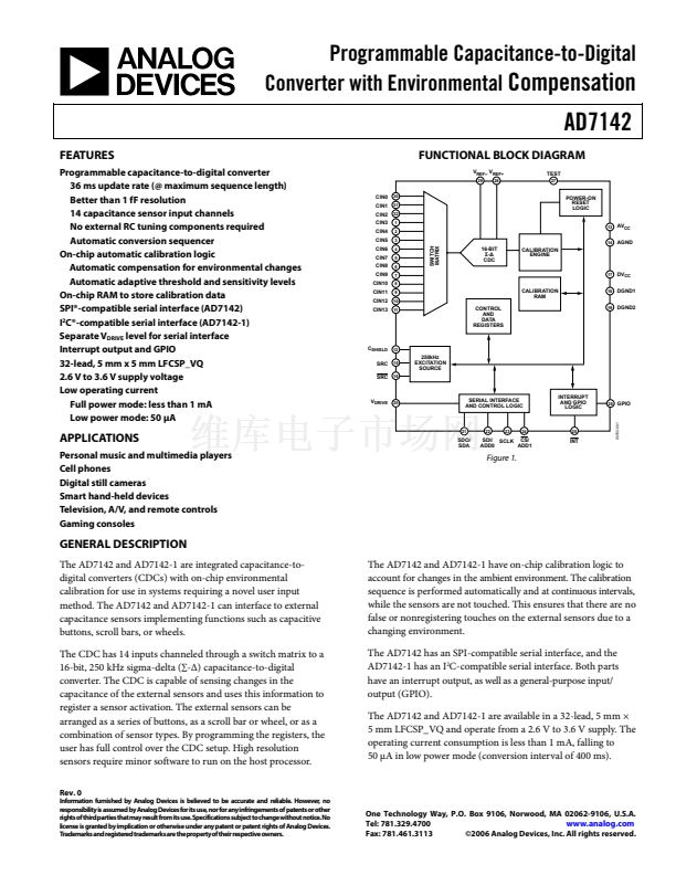
AD7142
t
CONV_FP
CDC
CONVERSION
CONVERSION
SEQUENCE N
CONVERSION
SEQUENCE N+1
CONVERSION
SEQUENCE N+2
05702-015
t
CONV_LP
CDC
CONVERSION
CONVERSION
SEQUENCE N
CONVERSION
SEQUENCE N+1
05702-016
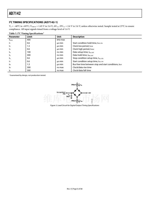
NOTES
1.
t
CONV_FP
= VALUE SET FROM TABLE 10.
NOTES
1.
t
CONV_LP
= t
CONV_FP
+ LP_CONV_DELAY
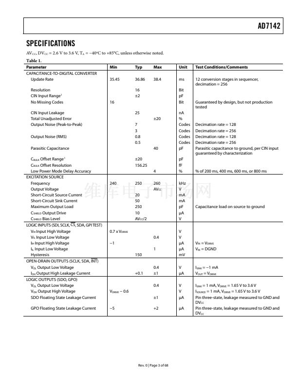
Figure 24. Full Power Mode CDC Conversion Sequence Time
Figure 25. Low Power Mode CDC Conversion Sequence Time
Low Power Mode CDC Conversion Sequence Time with
Delay
The frequency of each CDC conversion while operating in the
low power automatic wake up mode is controlled by using the
LP_CONV_DELAY register located at Address 0x000[3:2], in
addition to the registers listed in Table 10. This feature provides
some flexibility for optimizing the conversion time to meet
system requirements vs. AD7142 power consumption.
For example, maximum power savings is achieved when the
LP_CONV_DELAY register is set to 3. With a setting of 3, the
AD7142 automatically wakes up, performing a conversion every
800 ms.
Table 11. LP_CONV_DELAY Settings
LP_CONV_DELAY Bits
00
01
10
11
Delay Between Conversions
200 ms
400 ms
600 ms
800 ms
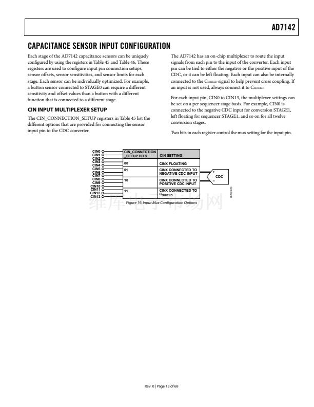
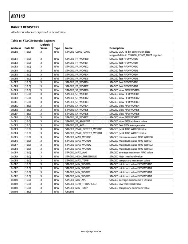
CDC CONVERSION RESULTS
Certain high resolution sensors require the host to read back
the CDC conversion results for processing. The registers
required for host processing are located in the Bank 3 registers.
The host processes the data readback from these registers using
a software algorithm, to determine position information.
In addition to the results registers in the Bank 3 registers, the
AD7142 provides the 16-bit CDC output data directly, starting
at Address 0x00B of Bank 1. Reading back the CDC 16-bit
conversion data register allows for customer-specific application
data processing.
Figure 25 shows a simplified timing example of the low power
CDC conversion time. As shown, the low power CDC
conversion time is set by t
CONV_FP
and the LP_CONV_DELAY
register.
Rev. 0 | Page 16 of 68


 1
1
 2
2
 3
3
 4
4
 5
5
 6
6
 7
7
 8
8
 9
9
 10
10
 11
11
 12
12
 13
13
 14
14
 15
15
 16
16
 17
17
 18
18
 19
19
 20
20
 21
21
 22
22
 23
23
 24
24
 25
25
 26
26
 27
27
 28
28
 29
29
 30
30
 31
31
 32
32
 33
33
 34
34
 35
35
 36
36
 37
37
 38
38
 39
39
 40
40
 41
41
 42
42
 43
43
 44
44
 45
45
 46
46
 47
47
 48
48
 49
49
 50
50
 51
51
 52
52
 53
53
 54
54
 55
55
 56
56
 57
57
 58
58
 59
59
 60
60
 61
61
 62
62
 63
63
 64
64
 65
65
 66
66
 67
67
 68
68
