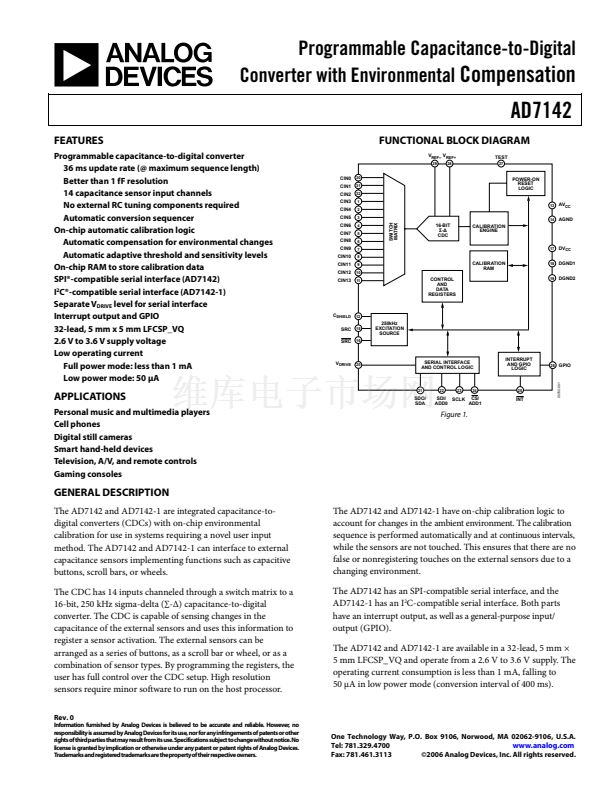
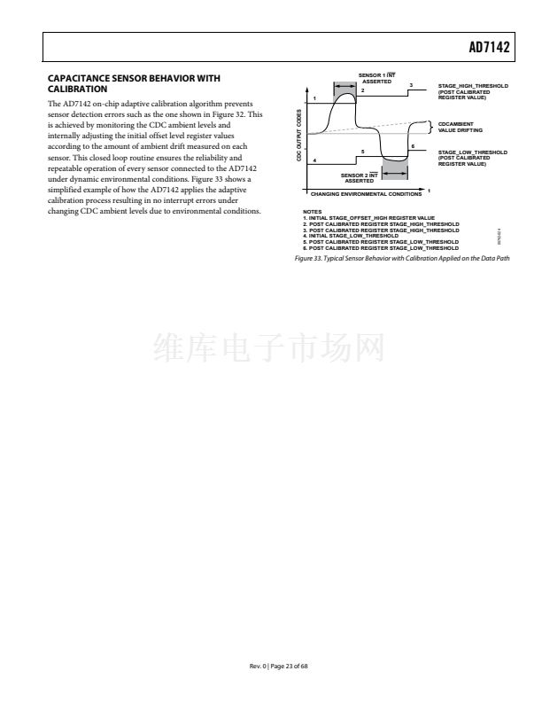
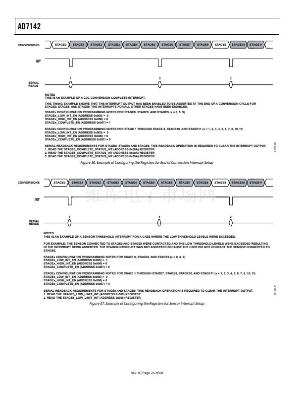
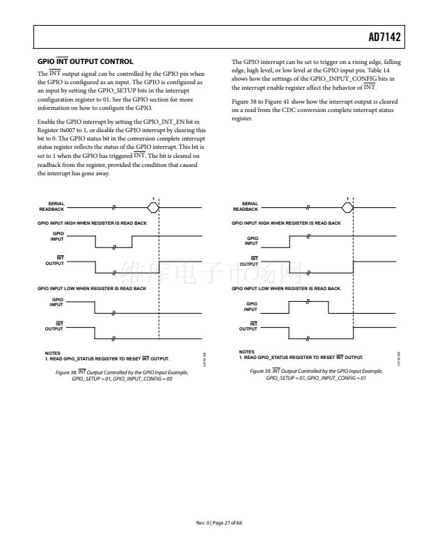
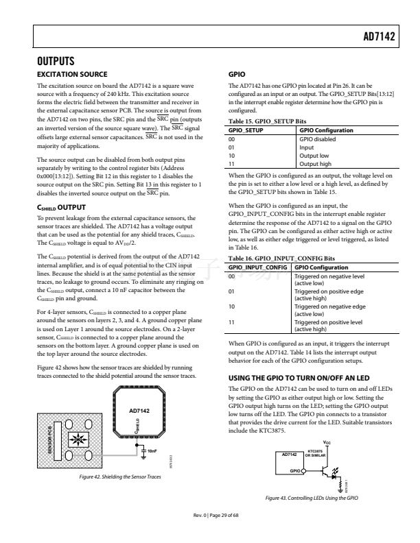
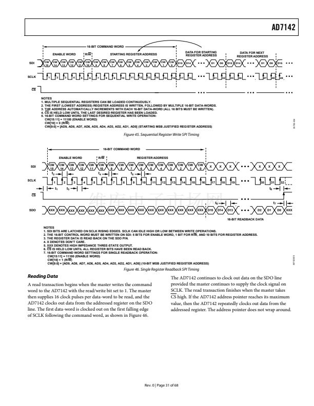
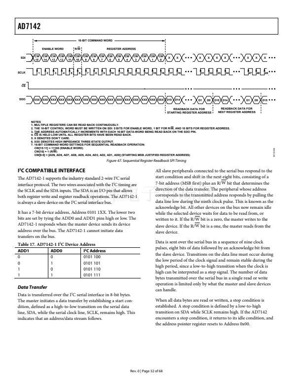
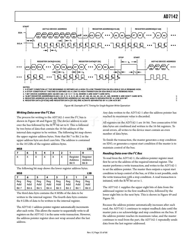
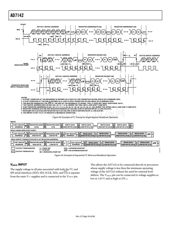
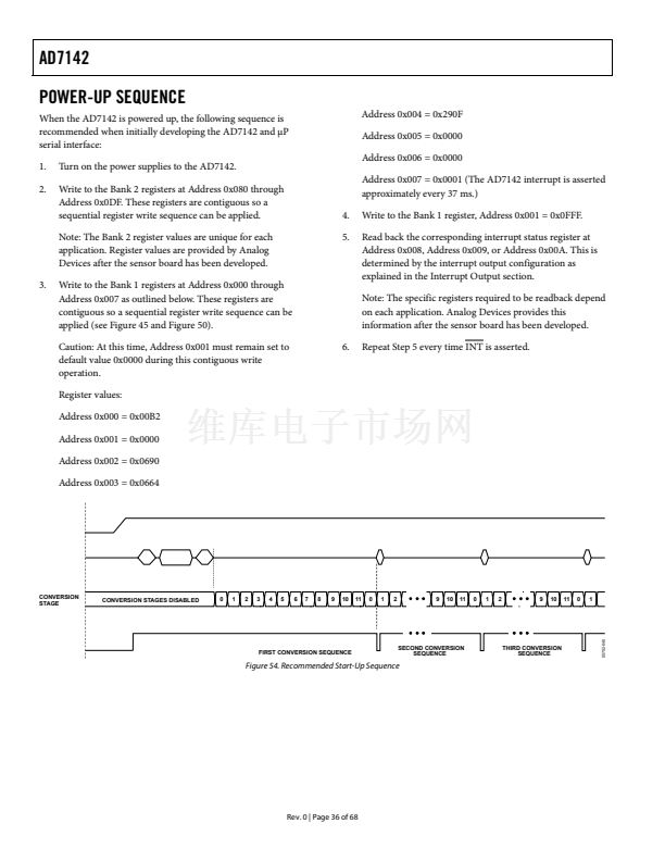
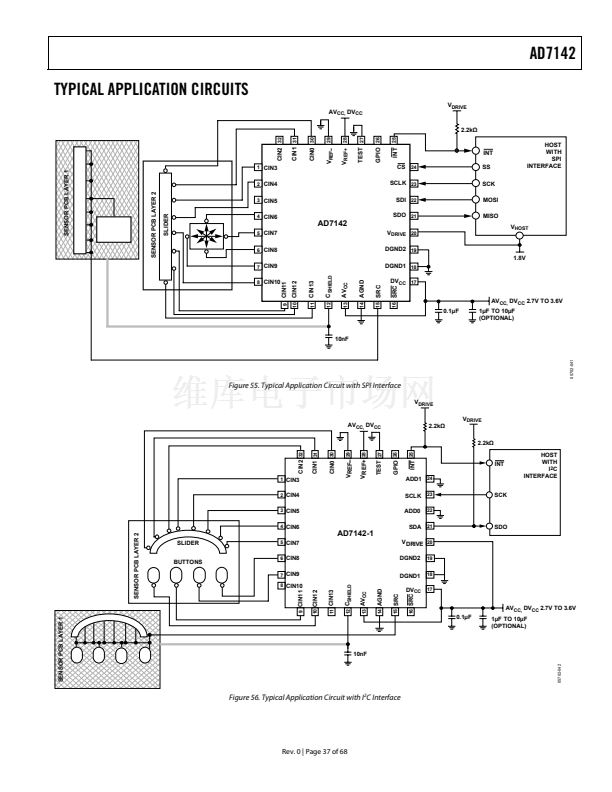
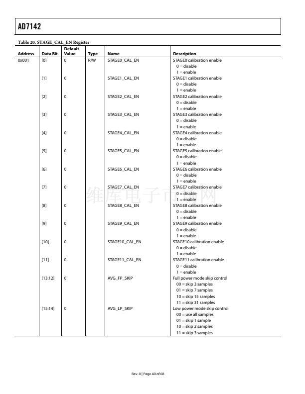
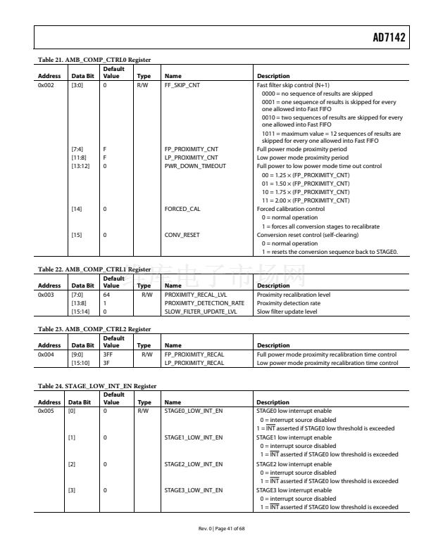
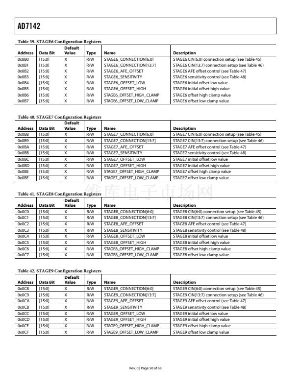
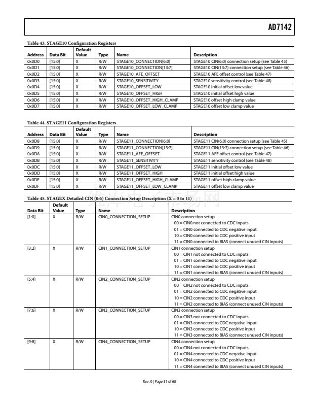
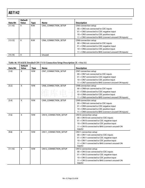
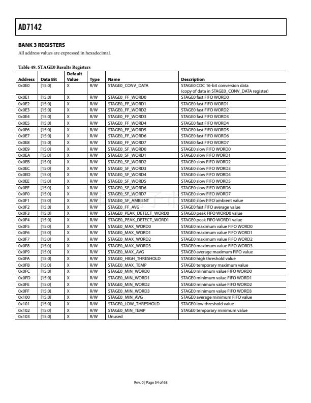
鈥?/div>
SENSOR
NEG_AFE_OFFSET_SWAP
REGISTER
EXT
鈥揇AC
(20pF RANGE)
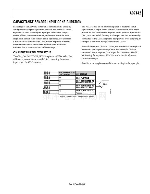
CIN_CONNECTION_SETUP
REGISTER
7
NEG_AFE_OFFSET
REGISTER
05702-011
Do not use this setting.
The decimation process on the AD7142 is an averaging process
where a number of samples are taken and the averaged result is
output. Due to the architecture of the digital filter employed, the
amount of samples taken (per stage) is equal to 3脳 the
decimation rate. So 3 脳 256 or 3 脳 128 samples are averaged to
obtain each stage result.
The decimation process reduces the amount of noise present in
the final CDC result. However, the higher the decimation rate,
the lower the output rate per stage, thus, a trade-off is possible
between a noise free signal and speed of sampling.
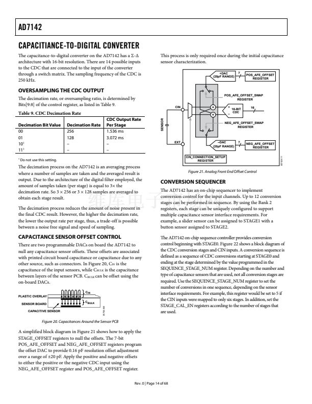
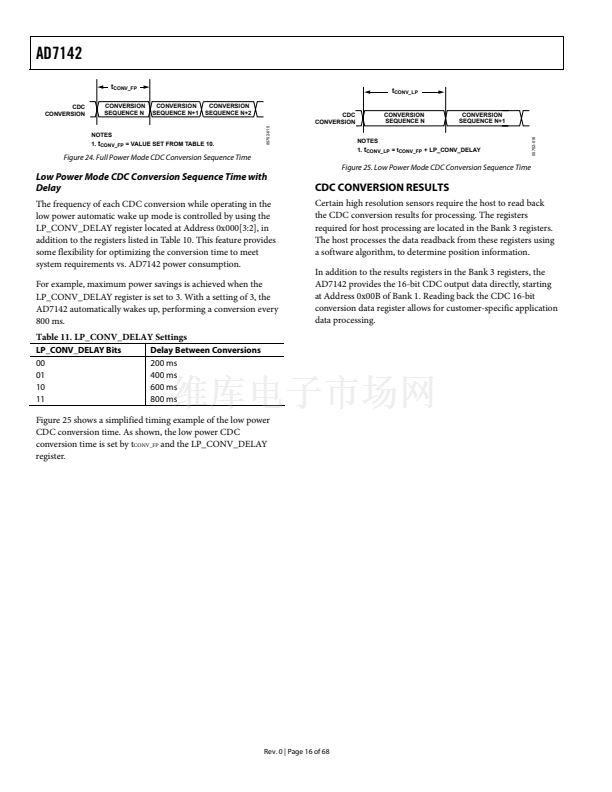
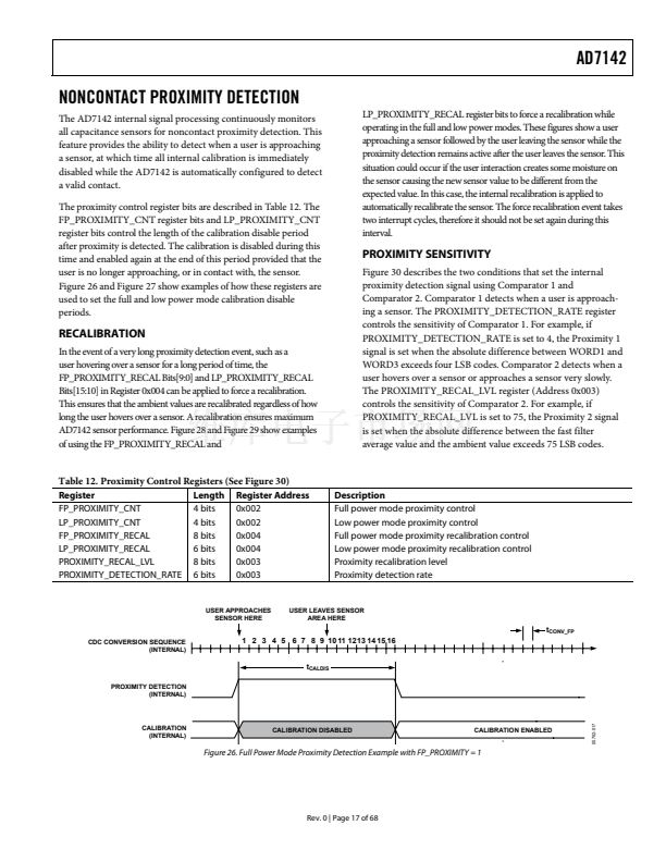
Figure 21. Analog Front End
Offset
Control
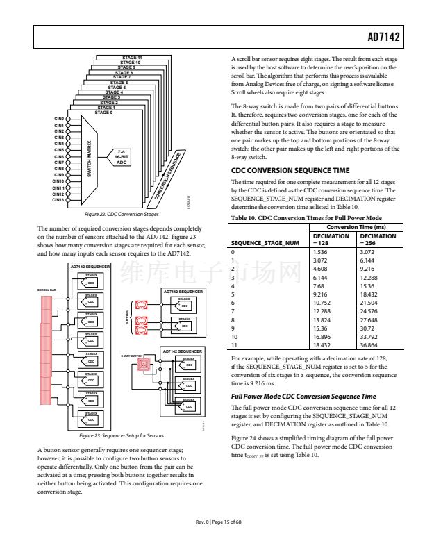
CONVERSION SEQUENCER
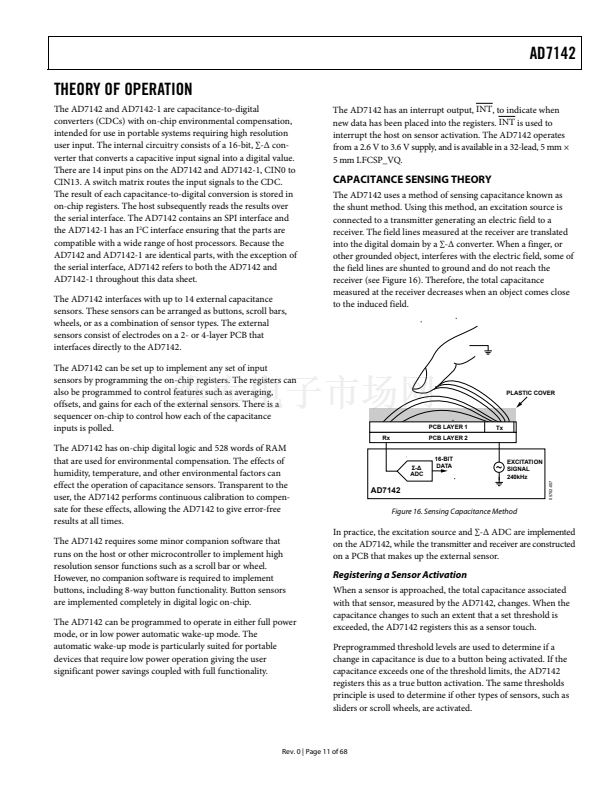
The AD7142 has an on-chip sequencer to implement
conversion control for the input channels. Up to 12 conversion
stages can be performed in sequence. By using the Bank 2
registers, each stage can be uniquely configured to support
multiple capacitance sensor interface requirements. For
example, a slider sensor can be assigned to STAGE1 with a
button sensor assigned to STAGE2.
The AD7142 on-chip sequence controller provides conversion
control beginning with STAGE0. Figure 22 shows a block diagram of
the CDC conversion stages and CIN inputs. A conversion sequence is
defined as a sequence of CDC conversions starting at STAGE0 and
ending at the stage determined by the value programmed in the
SEQUENCE_STAGE_NUM register. Depending on the number and
type of capacitance sensors that are used, not all conversion stages are
required. Use the SEQUENCE_STAGE_NUM register to set the
number of conversions in one sequence, depending on the sensor
interface requirements. For example, this register would be set to 5 if
the CIN inputs were mapped to only six stages. In addition, set the
STAGE_CAL_EN registers according to the number of stages that
are used.
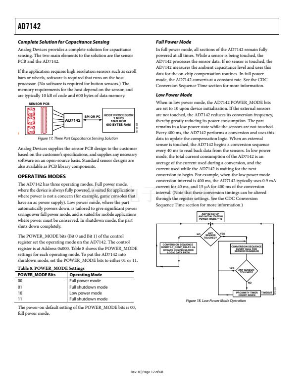
CAPACITANCE SENSOR OFFSET CONTROL
There are two programmable DACs on board the AD7142 to
null any capacitance sensor offsets. These offsets are associated
with printed circuit board capacitance or capacitance due to any
other source, such as connectors. In Figure 20, C
IN
is the
capacitance of the input sensors, while C
BULK
is the capacitance
between layers of the sensor PCB. C
BULK
can be offset using the
on-board DACs.
PLASTIC OVERLAY
SENSOR BOARD
CAPACITIVE SENSOR
C
IN
C
BULK
05702-054
Figure 20. Capacitances Around the Sensor PCB
A simplified block diagram in Figure 21 shows how to apply the
STAGE_OFFSET registers to null the offsets. The 7-bit
POS_AFE_OFFSET and NEG_AFE_OFFSET registers program
the offset DAC to provide 0.16 pF resolution offset adjustment
over a range of 鹵20 pF. Apply the positive and negative offsets
to either the positive or the negative CDC input using the
NEG_AFE_OFFSET register and POS_AFE_OFFSET register.
Rev. 0 | Page 14 of 68


 1
1
 2
2
 3
3
 4
4
 5
5
 6
6
 7
7
 8
8
 9
9
 10
10
 11
11
 12
12
 13
13
 14
14
 15
15
 16
16
 17
17
 18
18
 19
19
 20
20
 21
21
 22
22
 23
23
 24
24
 25
25
 26
26
 27
27
 28
28
 29
29
 30
30
 31
31
 32
32
 33
33
 34
34
 35
35
 36
36
 37
37
 38
38
 39
39
 40
40
 41
41
 42
42
 43
43
 44
44
 45
45
 46
46
 47
47
 48
48
 49
49
 50
50
 51
51
 52
52
 53
53
 54
54
 55
55
 56
56
 57
57
 58
58
 59
59
 60
60
 61
61
 62
62
 63
63
 64
64
 65
65
 66
66
 67
67
 68
68
