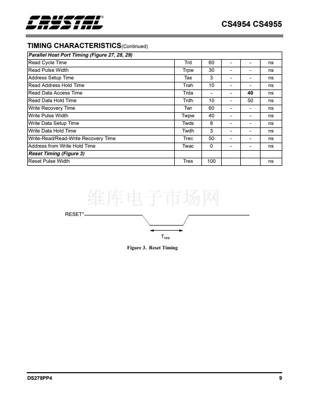
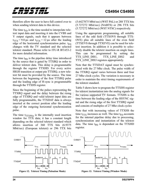
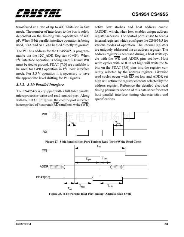
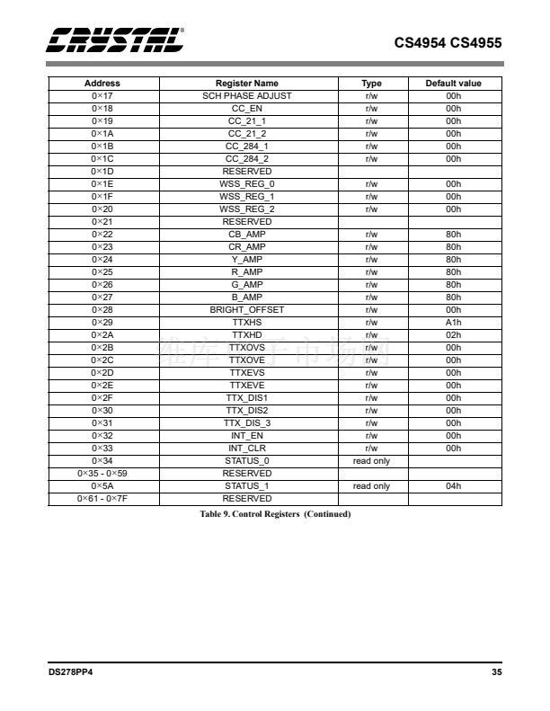
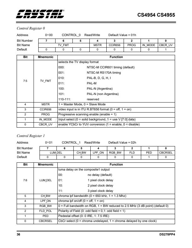
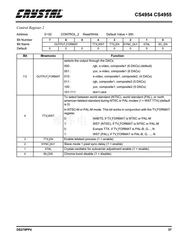
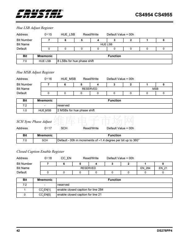
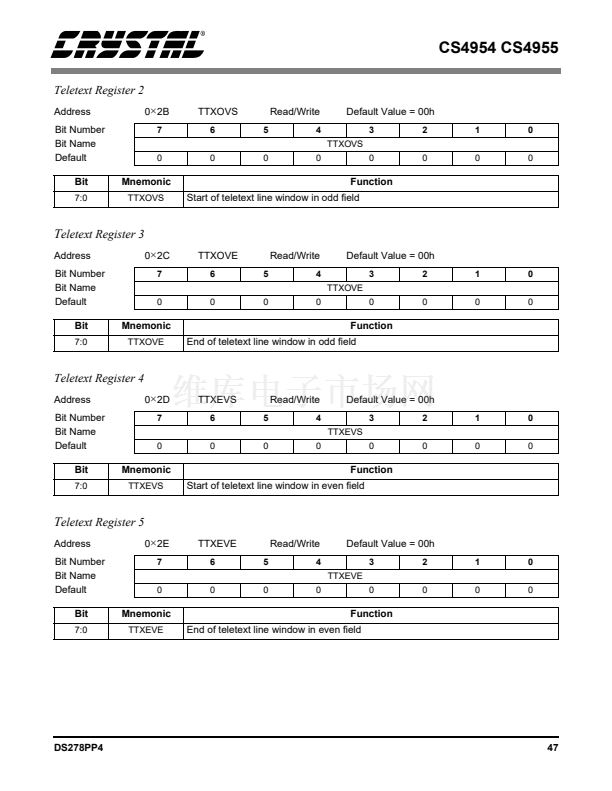
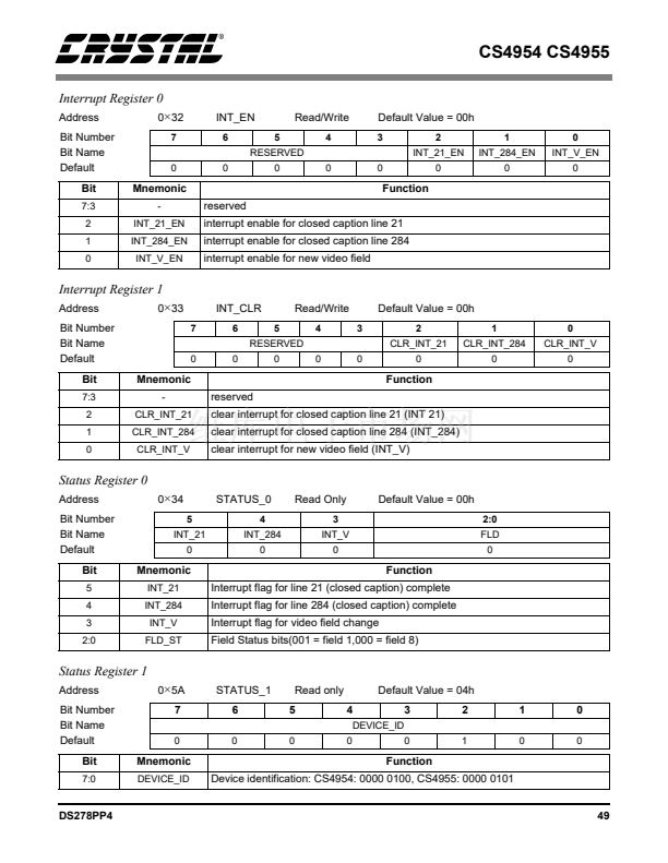
CS4954 CS4955
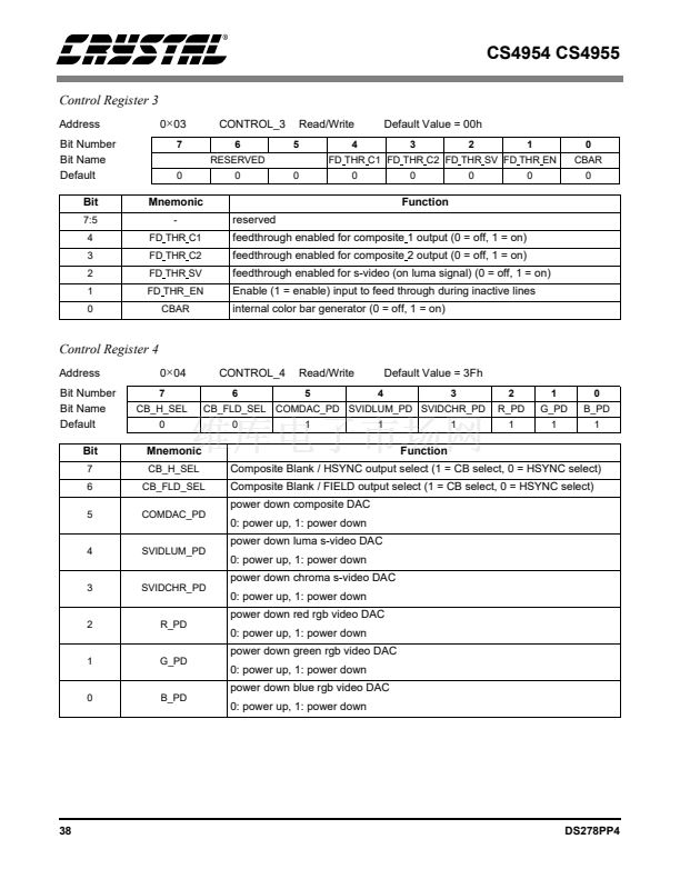
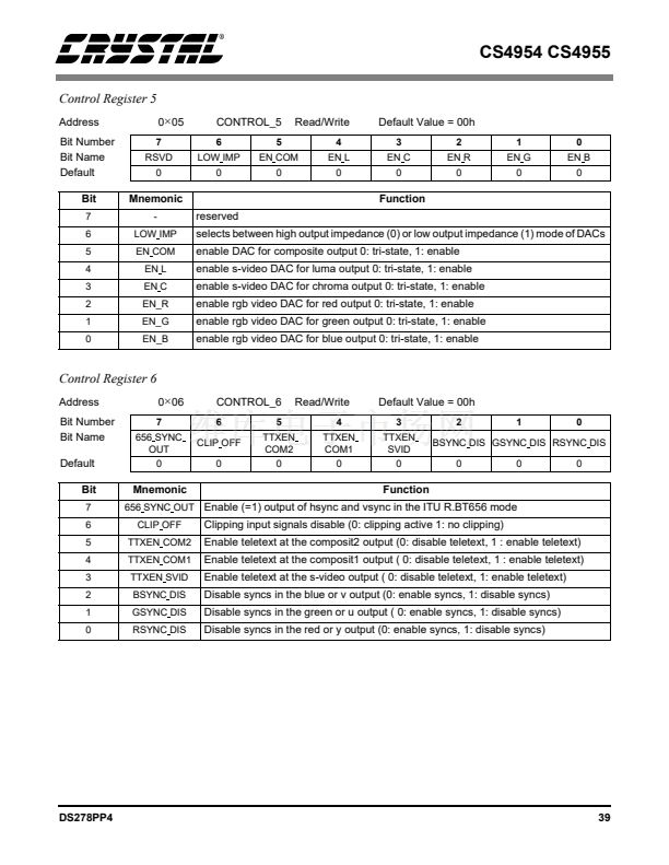
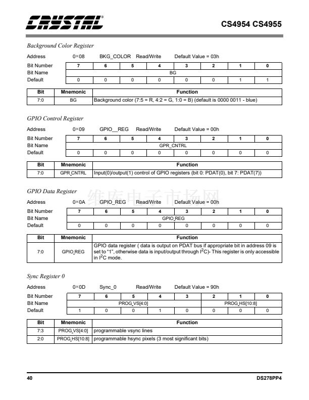
Background Color Register
Address
Bit Number
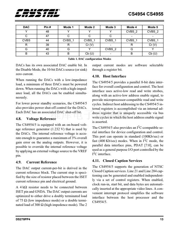
Bit Name
Default
Bit
7:0
0
脳
08
7
0
BKG_COLOR Read/Write
6
0
5
0
4
Default Value = 03h
3
BG
0
2
0
1
1
0
1
0
Mnemonic
BG
Function
Background color (7:5 = R, 4:2 = G, 1:0 = B) (default is 0000 0011 - blue)
GPIO Control Register
Address
Bit Number
Bit Name
Default
Bit
7:0
0
脳
09
7
0
GPIO__REG
6
0
5
0
Read/Write
4
0
Default Value = 00h
3
0
2
0
1
0
0
0
GPR_CNTRL
Mnemonic
GPR CNTRL
Function
Input(0)/output(1) control of GPIO registers (bit 0: PDAT(0), bit 7: PDAT(7))
GPIO Data Register
Address
Bit Number
Bit Name
Default
Bit
7:0
0
脳
0A
7
0
GPIO_REG
6
0
5
0
Read/Write
4
Default Value = 00h
3
GPIO REG
0
2
0
1
0
0
0
0
Mnemonic
GPIO REG
Function
GPIO data register ( data is output on PDAT bus if appropriate bit in address 09 is
set to 鈥?鈥? otherwise data is input/output through I
2
C)- This register is only accessible
in I
2
C mode.
Sync Register 0
Address
Bit Number
Bit Name
Default
Bit
7:3
2:0
0
脳
0D
7
1
Sync_0
6
0
5
Read/Write
4
1
PROG VS[4:0]
0
Default Value = 90h
3
0
2
0
1
PROG HS[10:8]
0
0
0
Mnemonic
PROG VS[4:0]
Function
programmable vsync lines
PROG HS[10:8]
programmable hsync pixels (3 most significant bits)
40
DS278PP4


 1
1
 2
2
 3
3
 4
4
 5
5
 6
6
 7
7
 8
8
 9
9
 10
10
 11
11
 12
12
 13
13
 14
14
 15
15
 16
16
 17
17
 18
18
 19
19
 20
20
 21
21
 22
22
 23
23
 24
24
 25
25
 26
26
 27
27
 28
28
 29
29
 30
30
 31
31
 32
32
 33
33
 34
34
 35
35
 36
36
 37
37
 38
38
 39
39
 40
40
 41
41
 42
42
 43
43
 44
44
 45
45
 46
46
 47
47
 48
48
 49
49
 50
50
 51
51
 52
52
 53
53
 54
54
 55
55
 56
56
