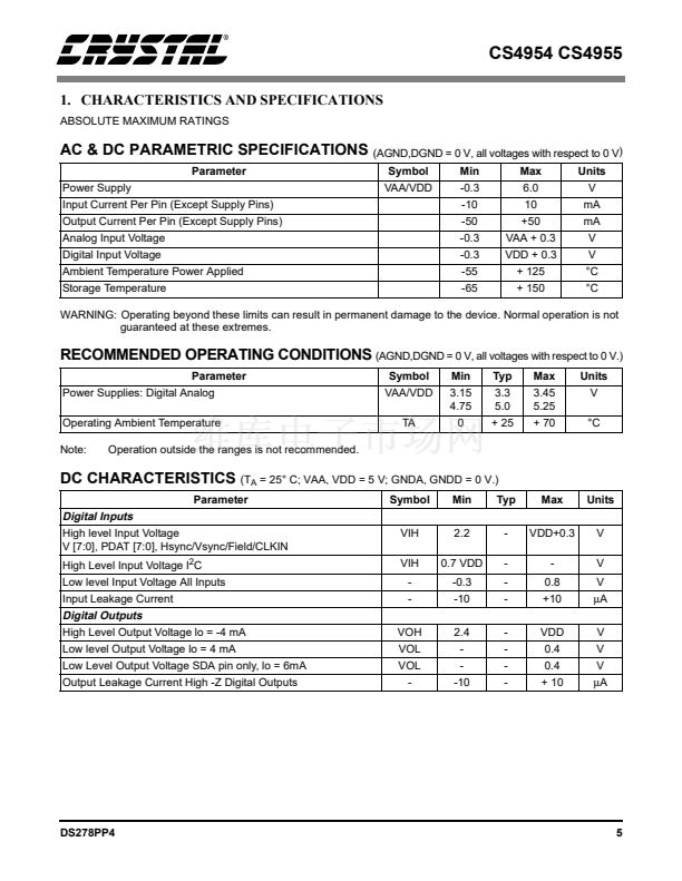
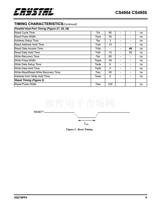
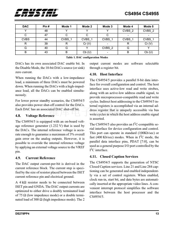
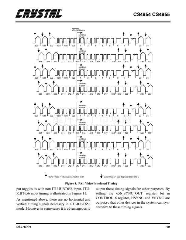
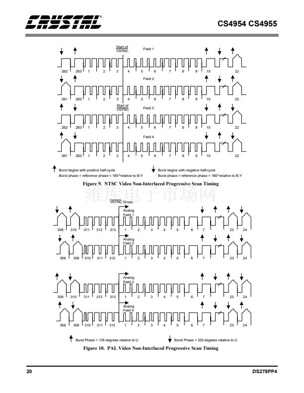
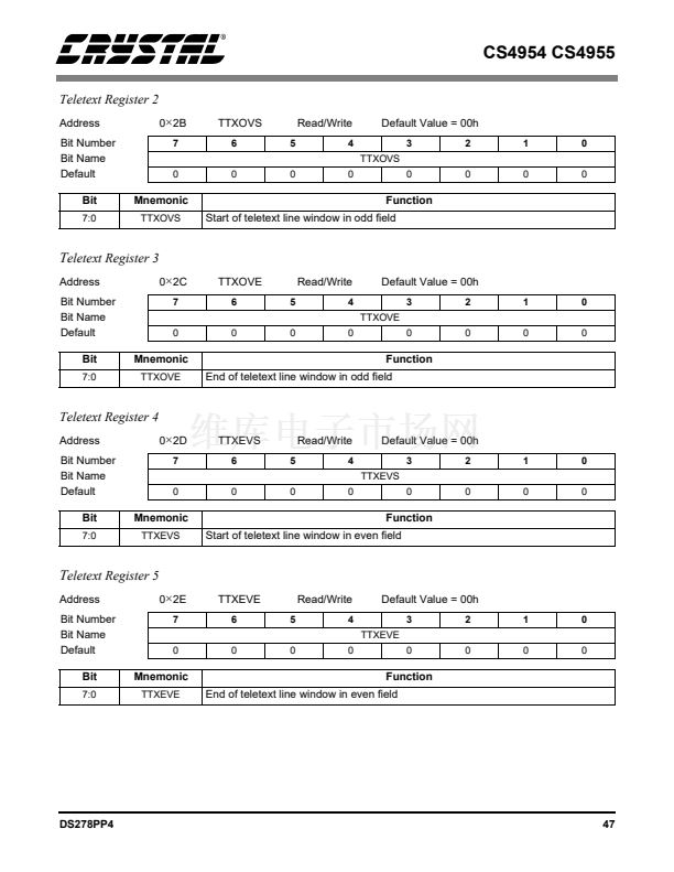
analog video specifications for NTSC and PAL.
(LOW_IMP but set to 1). The DAC output will
鈩?/div>
and
will output a video signal which conforms to the
analog video specifications for NTSC and PAL. No
external buffers are necessary, the ouputs can di-
rectly drive a television input.
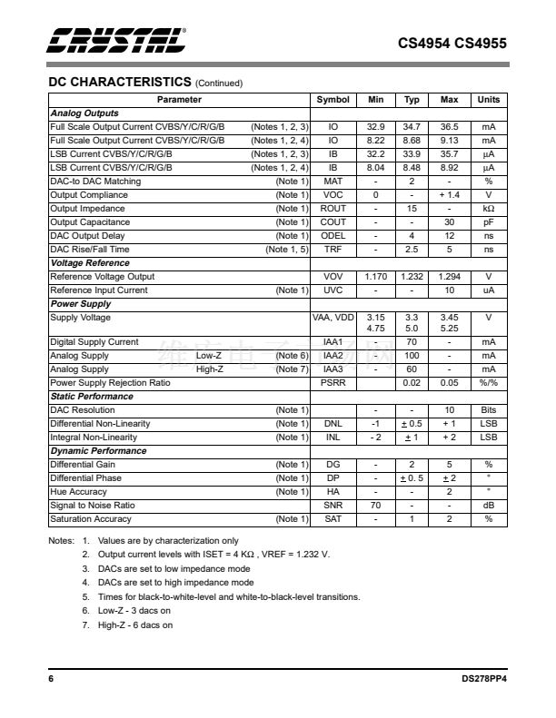
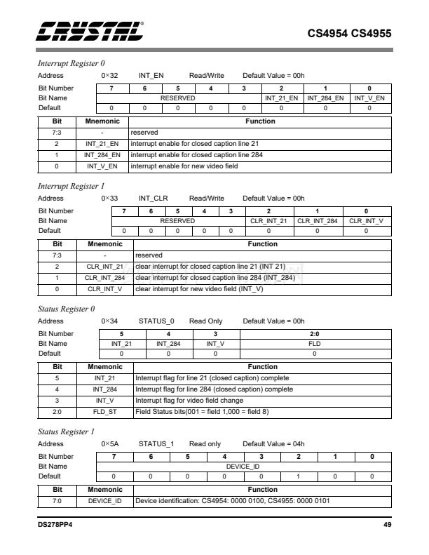
Note
that for power dissipation purposes it is not
always possible to have all the 6 DACs active at the
same time. Table 8 shows the maximum allowed
active DACs depending on the power supply and
low/high impedance modes. If less than 6 DACs
are allowed to be active the other ones
must
be
power down (see CONTROL_4 register).
Low/High
Impedance
mode
Low Impedance
High Impedance
Low Impedance
High Impedance
Nominal Power
supply
3.3V
3.3V
5.0V
5.0V
maximum # of
active DACs
3
6
3
6
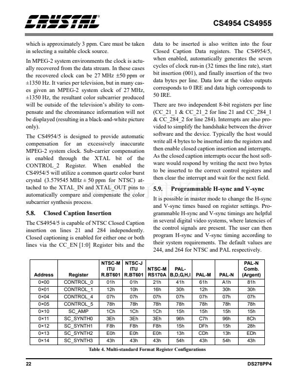
Table 8. Maximum DAC Numbers
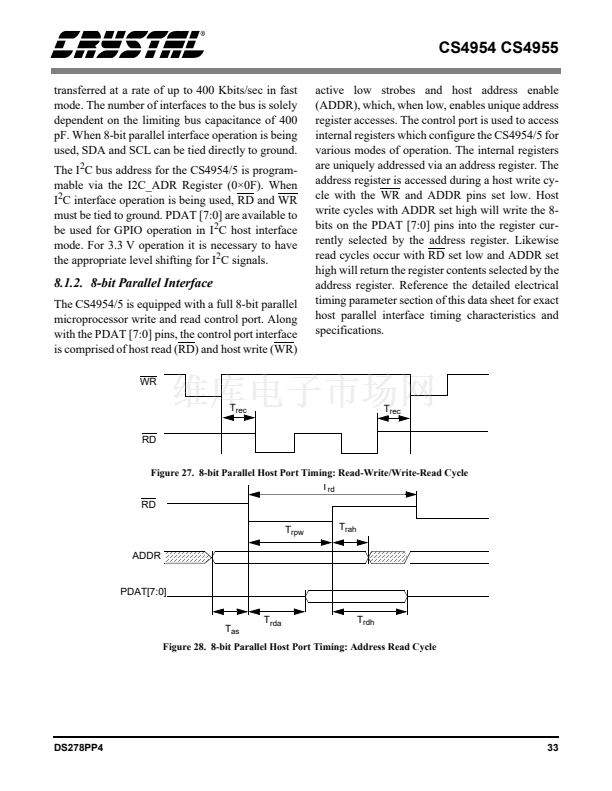
8.
8.1.
PROGRAMMING
Host Control Interface
The CS4954/5 host control interface can be config-
ured for I
2
C or 8-bit parallel operation. The
CS4954/5 will default to I
2
C operation when the
RD and WR pins are both tied low at power up. The
RD and WR pins are active for 8-bit parallel oper-
ation only.
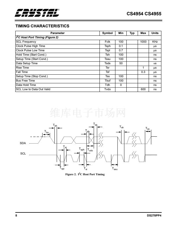
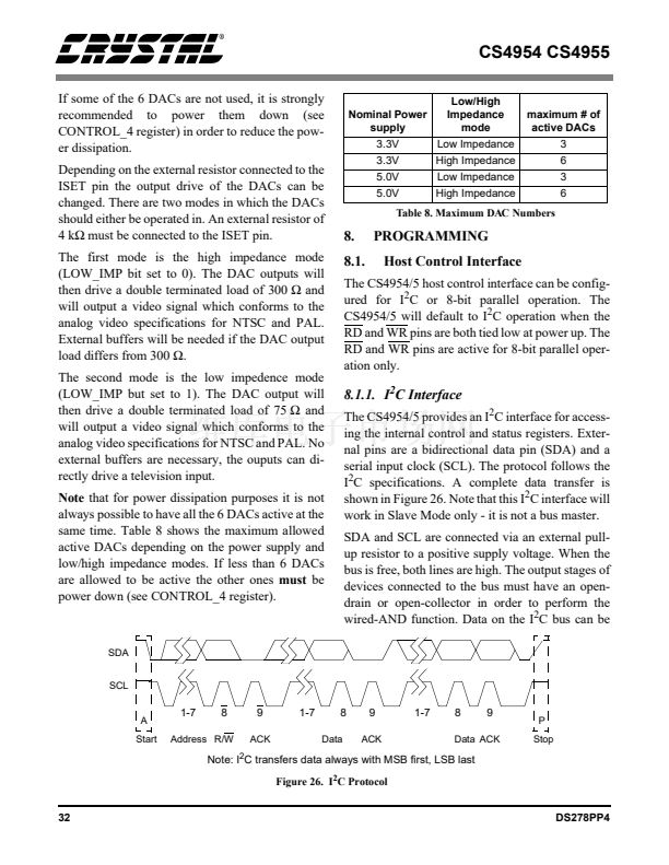
8.1.1. I
2
C Interface
The CS4954/5 provides an I
2
C interface for access-
ing the internal control and status registers. Exter-
nal pins are a bidirectional data pin (SDA) and a
serial input clock (SCL). The protocol follows the
I
2
C specifications. A complete data transfer is
shown in Figure 26. Note that this I
2
C interface will
work in Slave Mode only - it is not a bus master.
SDA and SCL are connected via an external pull-
up resistor to a positive supply voltage. When the
bus is free, both lines are high. The output stages of
devices connected to the bus must have an open-
drain or open-collector in order to perform the
wired-AND function. Data on the I
2
C bus can be
SDA
SCL
A
Start
1-7
8
9
ACK
1-7
8
Data
9
ACK
1-7
8
9
P
Stop
Address R/W
Data ACK
Note: I
2
C transfers data always with MSB first, LSB last
Figure 26. I
2
C Protocol
32
DS278PP4


 1
1
 2
2
 3
3
 4
4
 5
5
 6
6
 7
7
 8
8
 9
9
 10
10
 11
11
 12
12
 13
13
 14
14
 15
15
 16
16
 17
17
 18
18
 19
19
 20
20
 21
21
 22
22
 23
23
 24
24
 25
25
 26
26
 27
27
 28
28
 29
29
 30
30
 31
31
 32
32
 33
33
 34
34
 35
35
 36
36
 37
37
 38
38
 39
39
 40
40
 41
41
 42
42
 43
43
 44
44
 45
45
 46
46
 47
47
 48
48
 49
49
 50
50
 51
51
 52
52
 53
53
 54
54
 55
55
 56
56
