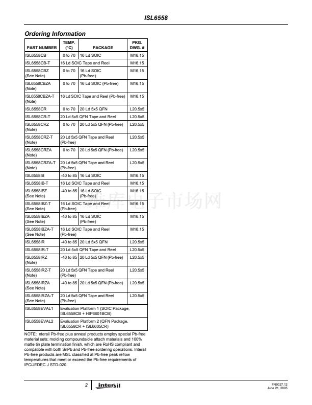
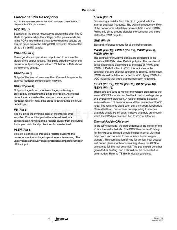
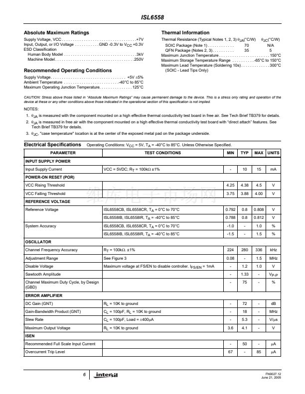
ISL6558
Operation
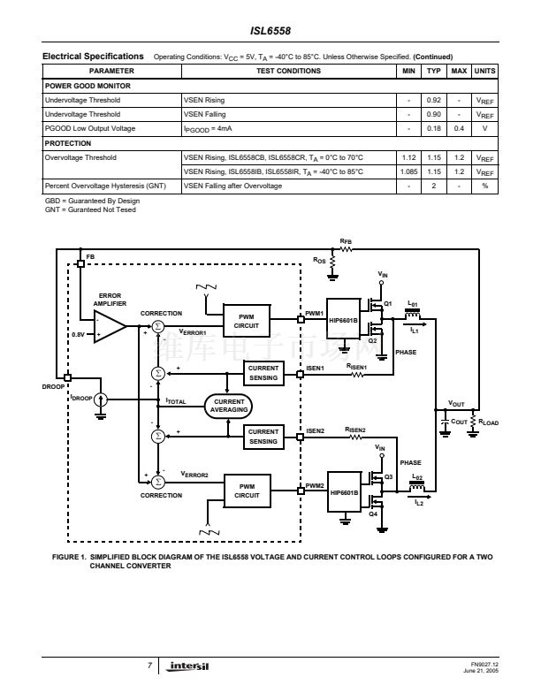
Figure 1 shows a simplified diagram of the voltage regulation
and current control loops for a two-phase converter. Both
voltage and current feedback are used to precisely regulate
output voltage and tightly control phase currents, I
L1
and I
L2
,
of the two power channels.
pulse width to lower the output current contribution by
Channel 2, while doing the opposite to Channel 1.
Droop Compensation
Microprocessors and other peripherals tend to change their
load current demands often from near no-load to full load
during operation. These same devices require minimal
output voltage deviation from nominal during a load step.
A high di/dt load step will cause an output voltage spike. The
amplitude of the spike is dictated by the output capacitor
ESR (effective series resistance) multiplied by the load step
magnitude and output capacitor ESL (equivalent series
inductance) times the load step di/dt. A positive load step
produces a negative output voltage spike and visa versa.
The overall output voltage deviation could exceed the
tolerance of some devices. One widely accepted solution to
this problem is output voltage 鈥渄roop鈥?or active voltage
positioning.
Droop is set relative to the output voltage tolerance
specifications of the load device. Most device tolerance
specifications straddle the nominal output voltage. At no-
load, the output voltage is set to a slightly higher than
nominal level, V
OUT,NL
. At full load, the output voltage is set
to a slightly lower than nominal level, V
OUT,FL
. The result is
a desire to have an output voltage characteristic as shown
by the load line in Figure 2.
V
OUT,NL
V
OUT,NOM
V
OUT,FL
Voltage Loop
Output voltage feedback is applied via the resistor
combination of R
FB
and R
OS
to the inverting input of the
error amplifier. This signal drives the error amplifier output
high or low, depending upon the scaled output voltage in
relation to the reference voltage of 0.8V. The amplifier output
voltage is distributed among the active PWM channels and
summed with their individual current correction signals. The
resultant signal, V
ERROR
, is fed into the PWM control
circuitry for each channel. Within this block, the signal is
compared with a sawtooth ramp signal. The sawtooth ramp
signal applied to each channel is out-of-phase with the
others. The resulting duty cycle signal for each channel is
determined by the movement of the correction voltage,
V
ERROR
, relative to the sawtooth ramp. The individual duty
cycle signals are sent to their respective HIP660x gate
drivers from the PWM pins. The HIP660x gate drivers then
switch their upper and lower MOSFETs in accordance to this
PWM signal.
Current Loop
The current control loop keeps the channel currents in
balance. During the PWM off-time of each channel, the
voltage developed across the r
DS(ON)
of the lower MOSFET
is sampled. The current is scaled by the R
ISEN
resistor and
provides feedback proportional to the output current of each
channel. The scaled output current from all active channels
are combined to create an average current reference,
I
TOTAL
, relative to the converter鈥檚 total output current. This
signal is then subtracted from the individual channel scaled
output currents to produce a current correction signal for
each channel. The current correction signal keeps each
channel鈥檚 output current contribution balanced relative to the
other active channels. Each current correction signal is then
subtracted from the error amplifier output and fed to the
individual channel PWM circuits.
For example, assume the voltage sampled across Q4 in
Figure 1 is higher than that sampled across Q2. The ISEN2
current would be higher then ISEN1. When the two
reference currents are averaged, they still accurately
represent the total output current of the converter. The
reference current I
TOTAL
is then subtracted from the ISEN
currents. This results in a positive offset for Channel 2 and a
negative offset for Channel 1. These offsets are subtracted
from the error amplifier signal and perform phase balance
correction. The V
ERROR2
signal is reduced, while V
ERROR1
would be increased. The PWM circuit would then reduce the
I
OUT,NL
NOMINAL LOAD LINE
I
OUT,MID
I
OUT,MAX
DROOP LOAD LINE
FIGURE 2. SIMPLE OUTPUT DEVICE LOAD LINE
With droop implemented and a positive load step, the
resulting negative output voltage spike begins from the slightly
elevated level of V
OUT,NL
. Similarly, if the load steps from full
load, I
OUT,MAX
, back to no-load, I
OUT,NL
, the output voltage
starts from the slightly lower V
OUT,FL
position. These few
millivolts of offset help reduce the size and cost of output
capacitors required to handle a given load step.
Droop is an optional feature of the ISL6558. It is
implemented by connecting the DROOP and FB pins as
shown in Figure 1. An internal current source, I
DROOP
,
feeds out of the DROOP pin. The magnitude of I
DROOP
is
controlled by the scaled representation of the total output
current created from the individual ISEN currents. I
DROOP
creates a voltage drop across R
FB
and offsets the output
8
FN9027.12
June 21, 2005


 1
1
 2
2
 3
3
 4
4
 5
5
 6
6
 7
7
 8
8
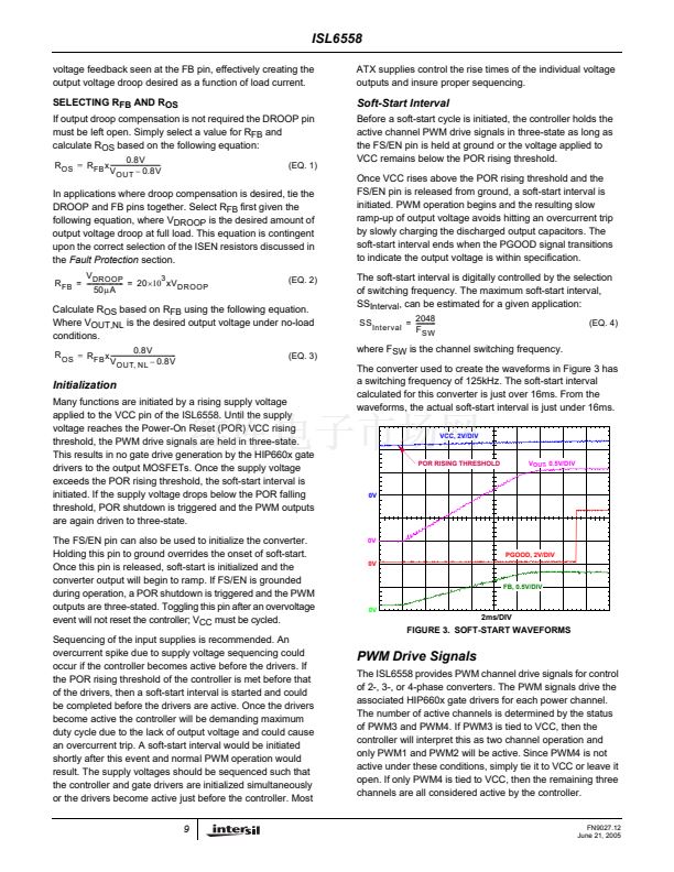 9
9
 10
10
 11
11
 12
12
 13
13
 14
14
 15
15
 16
16
