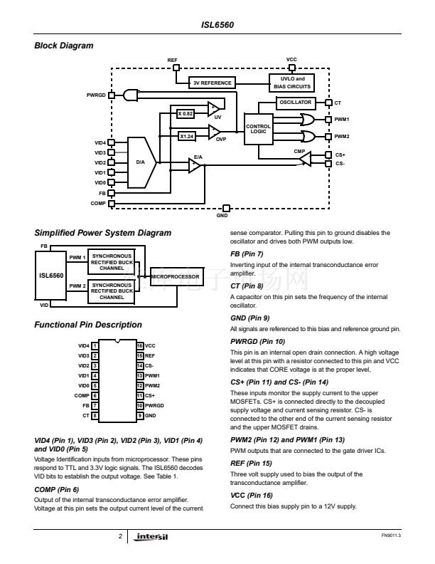
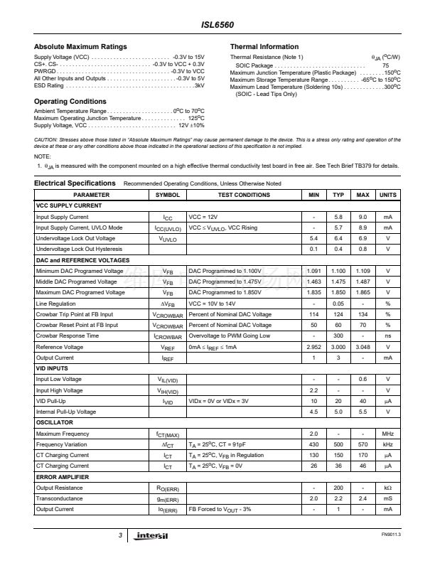
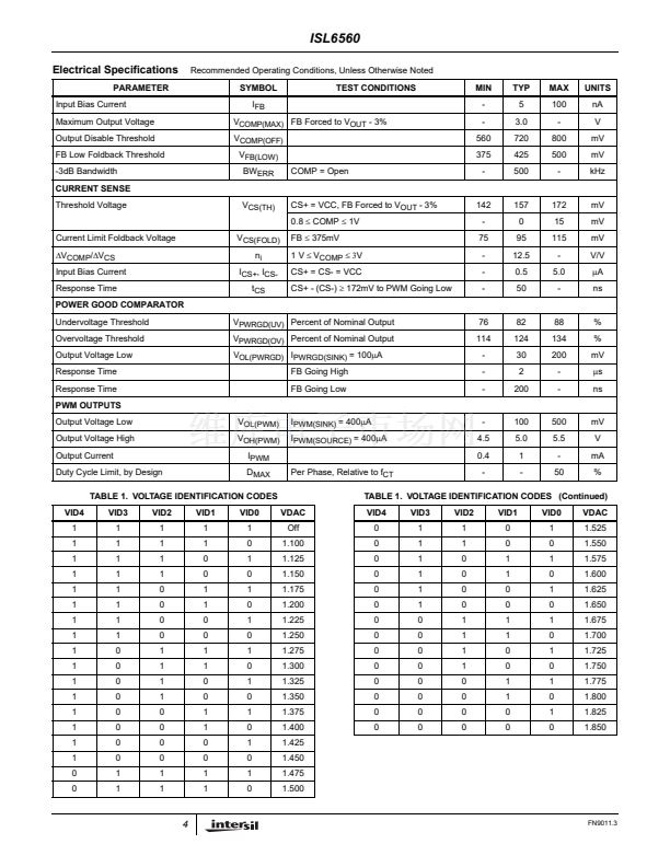
ISL6560
Absolute Maximum Ratings
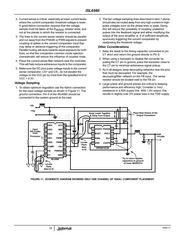
Supply Voltage (VCC) . . . . . . . . . . . . . . . . . . . . . . . . . -0.3V to 15V
CS+. CS- . . . . . . . . . . . . . . . . . . . . . . . . . . . . . -0.3V to VCC + 0.3V
PWRGD . . . . . . . . . . . . . . . . . . . . . . . . . . . . . . . . . . . . -0.3V to VCC
All Other Inputs and Outputs . . . . . . . . . . . . . . . . . . . . . . -0.3V to 5V
ESD Rating . . . . . . . . . . . . . . . . . . . . . . . . . . . . . . . . . . . . . . . . .3kV
Thermal Information
Thermal Resistance (Note 1)
胃
JA
(
o
C/W)
SOIC Package . . . . . . . . . . . . . . . . . . . . . . . . . . . . .
75
Maximum Junction Temperature (Plastic Package) . . . . . . . .150
o
C
Maximum Storage Temperature Range . . . . . . . . . . -65
o
C to 150
o
C
Maximum Lead Temperature (Soldering 10s) . . . . . . . . . . . . .300
o
C
(SOIC - Lead Tips Only)
Operating Conditions
Ambient Temperature Range . . . . . . . . . . . . . . . . . . . . . 0
o
C to 70
o
C
Maximum Operating Junction Temperature . . . . . . . . . . . . . . 125
o
C
Supply Voltage, VCC . . . . . . . . . . . . . . . . . . . . . . . . . . . . 12V
鹵10%
CAUTION: Stresses above those listed in 鈥淎bsolute Maximum Ratings鈥?may cause permanent damage to the device. This is a stress only rating and operation of the
device at these or any other conditions above those indicated in the operational sections of this specification is not implied.
NOTE:
1.
胃
JA
is measured with the component mounted on a high effective thermal conductivity test board in free air. See Tech Brief TB379 for details.
Electrical Specifications
PARAMETER
VCC SUPPLY CURRENT
Input Supply Current
Input Supply Current, UVLO Mode
Undervoltage Lock Out Voltage
Undervoltage Lock Out Hysteresis
Recommended Operating Conditions, Unless Otherwise Noted
SYMBOL
TEST CONDITIONS
MIN
TYP
MAX
UNITS
I
CC
I
CC(UVLO)
V
UVLO
VCC = 12V
VCC
鈮?/div>
V
UVLO
, VCC Rising
-
-
5.4
0.1
5.8
5.7
6.4
0.4
9.0
8.9
6.9
0.8
mA
mA
V
V
DAC and REFERENCE VOLTAGES
Minimum DAC Programed Voltage
Middle DAC Programed Voltage
Maximum DAC Programed Voltage
Line Regulation
Crowbar Trip Point at FB Input
Crowbar Reset Point at FB Input
Crowbar Response Time
Reference Voltage
Output Current
VID INPUTS
Input Low Voltage
Input High Voltage
VID Pull-Up
Internal Pull-Up Voltage
OSCILLATOR
Maximum Frequency
Frequency Variation
CT Charging Current
CT Charging Current
ERROR AMPLIFIER
Output Resistance
Transconductance
Output Current
R
O(ERR)
g
m(ERR)
Io
(ERR)
FB Forced to V
OUT
- 3%
-
2.0
-
200
2.2
1
-
2.4
-
k鈩?/div>
mS
mA
f
CT(MAX)
鈭唂
CT
I
CT
I
CT
T
A
= 25
o
C, CT = 91pF
T
A
= 25
o
C, V
FB
in Regulation
T
A
= 25
o
C, V
FB
= 0V
2.0
430
130
26
-
500
150
36
-
570
170
46
MHz
kHz
碌A(chǔ)
碌A(chǔ)
V
IL(VID)
V
IH(VID)
I
VID
VIDx = 0V or VIDx = 3V
-
2.2
10
4.5
-
-
20
5.0
0.6
-
40
5.5
V
V
碌A(chǔ)
V
V
FB
V
FB
V
FB
鈭哣
FB
V
CROWBAR
V
CROWBAR
I
CROWBAR
V
REF
I
REF
DAC Programmed to 1.100V
DAC Programmed to 1.475V
DAC Programmed to 1.850V
VCC = 10V to 14V
Percent of Nominal DAC Voltage
Percent of Nominal DAC Voltage
Overvoltage to PWM Going Low
0mA
鈮?/div>
I
REF
鈮?/div>
1mA
1.091
1.463
1.835
-
114
50
-
2.952
1
1.100
1.475
1.850
0.05
124
60
300
3.000
3
1.109
1.487
1.865
-
134
70
-
3.048
-
V
V
V
%
%
%
ns
V
mA
3
FN9011.3


 1
1
 2
2
 3
3
 4
4
 5
5
 6
6
 7
7
 8
8
 9
9
 10
10
 11
11
 12
12
 13
13
 14
14
