ISL6560
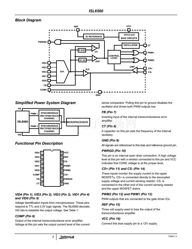
Block Diagram
REF
VCC
3V REFERENCE
PWRGD
UVLO and
BIAS CIRCUITS
OSCILLATOR
CT
PWM1
CONTROL
LOGIC
PWM2
CMP
+
X 0.82
-
UV
+
X1.24
VID4
VID3
VID2
VID1
VID0
FB
COMP
D/A
E/A
+
-
OVP
+
CS+
CS-
-
-
GND
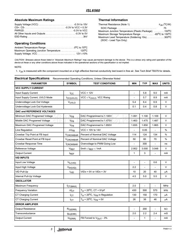
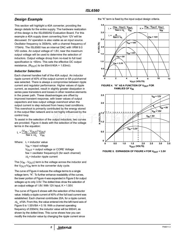
Simplified Power System Diagram
FB
PWM 1
SYNCHRONOUS
RECTIFIED BUCK
CHANNEL
MICROPROCESSOR
PWM 2
SYNCHRONOUS
RECTIFIED BUCK
CHANNEL
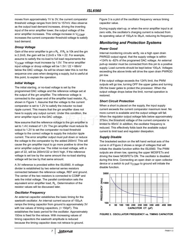
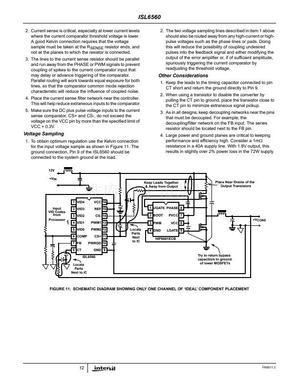
sense comparator. Pulling this pin to ground disables the
oscillator and drives both PWM outputs low.
FB (Pin 7)
Inverting input of the internal transconductance error
amplifier.
ISL6560
CT (Pin 8)
A capacitor on this pin sets the frequency of the internal
oscillator.
VID
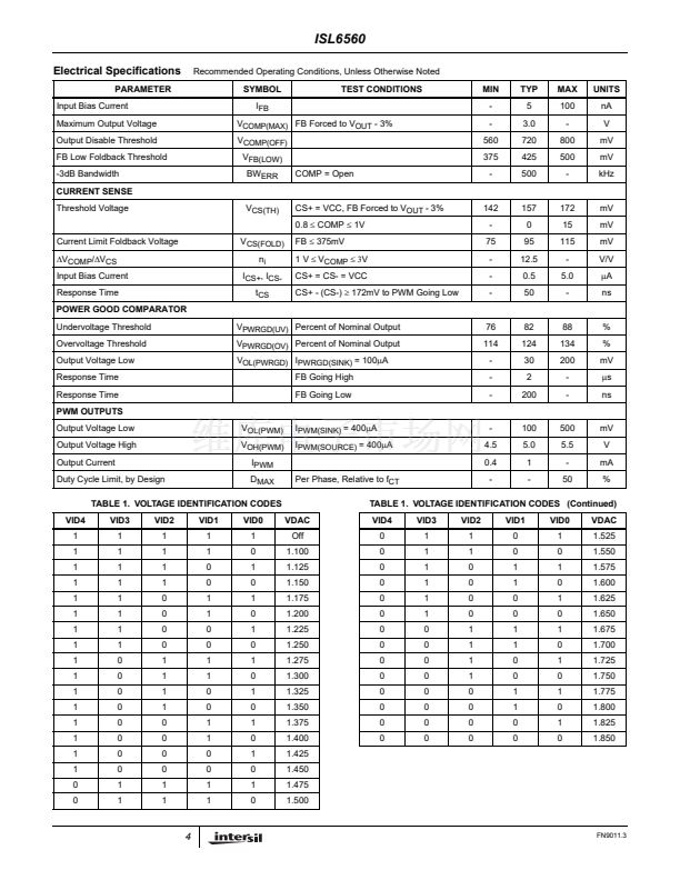
Functional Pin Description
VID4 1
VID3 2
VID2 3
VID1 4
VID0 5
COMP 6
FB 7
CT 8
16 VCC
15 REF
14 CS-
13 PWM1
12 PWM2
11 CS+
10 PWRGD
9 GND
GND (Pin 9)
All signals are referenced to this bias and reference ground pin.
PWRGD (Pin 10)
This pin is an internal open drain connection. A high voltage
level at this pin with a resistor connected to this pin and VCC
indicates that CORE voltage is at the proper level,
CS+ (Pin 11) and CS- (Pin 14)
These inputs monitor the supply current to the upper
MOSFETs. CS+ is connected directly to the decoupled
supply voltage and current sensing resistor. CS- is
connected to the other end of the current sensing resistor
and the upper MOSFET drains.
VID4 (Pin 1), VID3 (Pin 2), VID2 (Pin 3), VID1 (Pin 4)
and VID0 (Pin 5)
Voltage Identification inputs from microprocessor. These pins
respond to TTL and 3.3V logic signals. The ISL6560 decodes
VID bits to establish the output voltage. See Table 1.
PWM2 (Pin 12) and PWM1 (Pin 13)
PWM outputs that are connected to the gate driver ICs.
REF (Pin 15)
Three volt supply used to bias the output of the
transconductance amplifier.
COMP (Pin 6)
Output of the internal transconductance error amplifier.
Voltage at this pin sets the output current level of the current
VCC (Pin 16)
Connect this bias supply pin to a 12V supply.
2
FN9011.3


 1
1
 2
2
 3
3
 4
4
 5
5
 6
6
 7
7
 8
8
 9
9
 10
10
 11
11
 12
12
 13
13
 14
14
