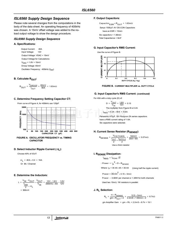
FIGURE 8. EQUATIONS TO DETERMINE R
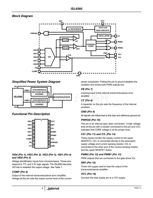
output of the transconductance error amplifier.
. This yields
1.63m鈩?/div>
脳
9mF
-
-
C
C
= -------------------------------------- = ---------------------------------------- =
1.68nF
8.7k
R
L
The ni term is the ratio of the V
COMP
to the current
comparator threshold voltage; see Figure 2. R
L
is made up
of two resistors that form a voltage divider from the internal
3V reference supply.
As described earlier in the
Circuit Description
section, the
output voltage of the gm amplifier establishes the threshold
voltage of the current comparator. At approximately 1V, the
current comparator threshold voltage is near zero. With no
current demands, the regulator output voltage would be the
same as the programmed DAC voltage. However, an 8A
ripple current was selected for this design. This results in the
output of the gm amplifier moving upwards to supply the
ripple current. The voltage at the COMP pin, V
SET
, will be:
I
RIPPLE
脳
R
SENSE
脳
ni
V
SET
=
1V
+ ---------------------------------------------------------------
-
2
8A
脳
5m鈩?/div>
脳
12.5
=
1V
+ --------------------------------------------- =
1V
+
250mV
=
1.25V
2
The voltage divider establishes the reference voltage for
V
COMP
that was set to 1.2V for this design, so the error
amplifier must drive the COMP pin 50mV more positive to
bring it to 1.25V from the 1.2V originally set. This additional
50mV output will result in an input voltage to the error
amplifier of: 50mv / 19.1 = 2.62mV below the programmed
DAC voltage of 1.8V. Neglected, is a negative term
associated with the 60ns delay of the current comparator.
This delay will cause the current ramp to be slightly greater
than predicted by the equation. This means that the initial
setting should be slightly reduced to account for the increase
in current.
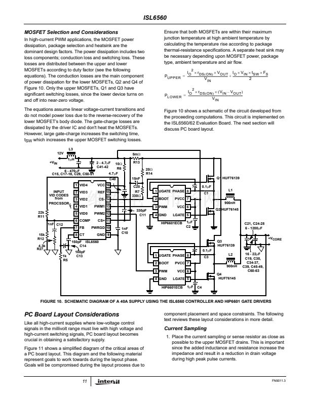
A 1nF capacitor was selected from transient testing. To
prevent excessive phase shift due to the compensation
capacitor, it is usually necessary to place a resistor inseries
with the capacitor to prevent excessive phase shift beyond
the frequency of interest. This is pole cancellation and the
resistor is approximately 0.5 x R
L
. Figure 9 shows this
network and the equivalent circuit is approximately 0.5 x R
L
.
Many variables have been used in the selection of the
various gain and filter networks to this point. A broad range
of component tolerances range from
鹵
1% to
鹵
20% have
been used in the design. Therefore, it is important to
evaluate the entire system with dynamic pulse load testing.
This will verify optimum transient response and also indicate
poor response in terms of excessive overshoot, ringing or
oscillation if the compensation network is not optimum.
V
REF = 3V
AC Equivalent
RU
C
C
R
C
C
C
R
C
R
L
To COMP pin
R
B
R
C
= 0.5 x R
L
FIGURE 9. COMPENSATION CIRCUIT
10
FN9011.3


 1
1
 2
2
 3
3
 4
4
 5
5
 6
6
 7
7
 8
8
 9
9
 10
10
 11
11
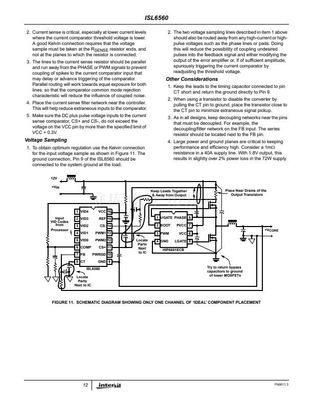 12
12
 13
13
 14
14
