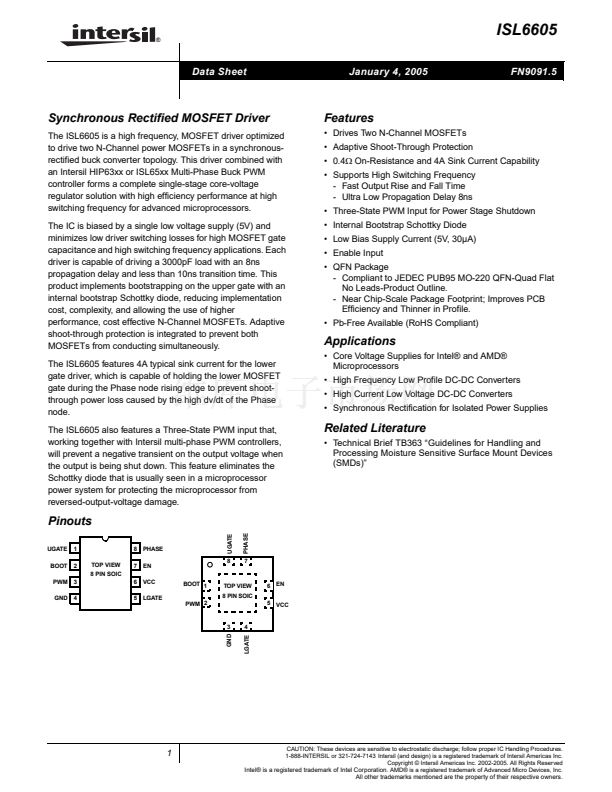
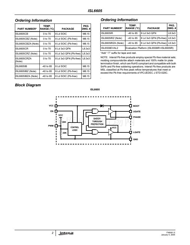
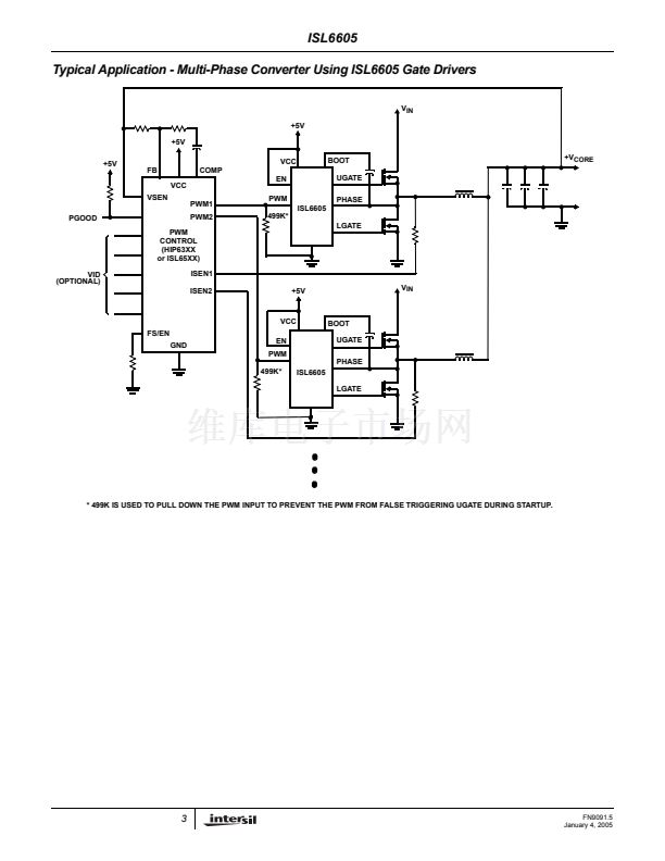
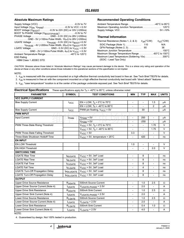
ISL6605
This driver is optimized for voltage regulators with large step
down ratio. The lower MOSFET is usually sized much larger
compared to the upper MOSFET because the lower
MOSFET conducts for a much longer time in a switching
period. The lower gate driver is therefore sized much larger
to meet this application requirement. The 0.4鈩?on-resistance
and 4A sink current capability enable the lower gate driver to
absorb the current injected to the lower gate through the
drain-to-gate capacitor of the lower MOSFET and prevent a
shoot through caused by the high dv/dt of the phase node.
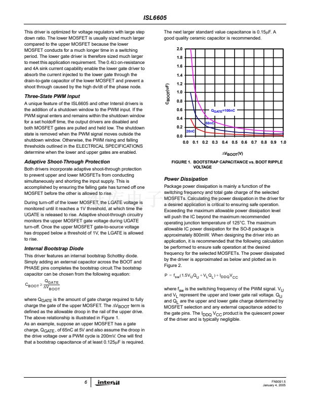
The next larger standard value capacitance is 0.15碌F. A
good quality ceramic capacitor is recommended.
2.0
2.0
1.8
1.8
1.6
1.6
1.4
1.4
1.2
1.2
1.0
1.0
0.8
0.8
0.6
0.6
0.4
0.4
0.2
0.2
0.0
C
BOOT
(uF)
Three-State PWM Input
A unique feature of the ISL6605 and other Intersil drivers is
the addition of a shutdown window to the PWM input. If the
PWM signal enters and remains within the shutdown window
for a set holdoff time, the output drivers are disabled and
both MOSFET gates are pulled and held low. The shutdown
state is removed when the PWM signal moves outside the
shutdown window. Otherwise, the PWM rising and falling
thresholds outlined in the ELECTRICAL SPECIFICATIONS
determine when the lower and upper gates are enabled.
Q
GATE
= 100 nC
Q
GATE
=100nC
50nC
20nC
20nC
50nC
0.0
0.0 0.1 0.2 0.3 0.4 0.5 0.6 0.7 0.8 0.9 1.0
0.0 0.1 0.2 0.3 0.4 0.5 0.6 0.7 0.8 0.9 1.0
鈭哣
BOOT
(V)
FIGURE 1. BOOTSTRAP CAPACITANCE vs. BOOT RIPPLE
VOLTAGE
Adaptive Shoot-Through Protection
Both drivers incorporate adaptive shoot-through protection
to prevent upper and lower MOSFETs from conducting
simultaneously and shorting the input supply. This is
accomplished by ensuring the falling gate has turned off one
MOSFET before the other is allowed to rise.
During turn-off of the lower MOSFET, the LGATE voltage is
monitored until it reaches a 1V threshold, at which time the
UGATE is released to rise. Adaptive shoot-through circuitry
monitors the upper MOSFET gate voltage during UGATE
turn-off. Once the upper MOSFET gate-to-source voltage
has dropped below a threshold of 1V, the LGATE is allowed
to rise.
Power Dissipation
Package power dissipation is mainly a function of the
switching frequency and total gate charge of the selected
MOSFETs. Calculating the power dissipation in the driver for
a desired application is critical to ensuring safe operation.
Exceeding the maximum allowable power dissipation level
will push the IC beyond the maximum recommended
operating junction temperature of 125擄C. The maximum
allowable IC power dissipation for the SO-8 package is
approximately 800mW. When designing the driver into an
application, it is recommended that the following calculation
be performed to ensure safe operation at the desired
frequency for the selected MOSFETs. The power dissipated
by the driver is approximated as below and plotted as in
Figure 2.
P
=
f
sw
(
1.5V
U
Q
+
V
L
Q
)
+
I
DDQ
V
U
L
CC
Internal Bootstrap Diode
This driver features an internal bootstrap Schottky diode.
Simply adding an external capacitor across the BOOT and
PHASE pins completes the bootstrap circuit.The bootstrap
capacitor can be chosen from the following equation:
Q
GATE
-
C
BOOT
鈮?/div>
-----------------------
鈭哣
BOOT
where Q
GATE
is the amount of gate charge required to fully
charge the gate of the upper MOSFET. The
鈭哣
BOOT
term is
defined as the allowable droop in the rail of the upper drive.
The above relationship is illustrated in Figure 1.
As an example, suppose an upper MOSFET has a gate
charge, Q
GATE
, of 65nC at 5V and also assume the droop in
the drive voltage over a PWM cycle is 200mV. One will find
that a bootstrap capacitance of at least 0.125碌F is required.
where f
sw
is the switching frequency of the PWM signal. V
U
and V
L
represent the upper and lower gate rail voltage. Q
U
and Q
L
are the upper and lower gate charge determined by
MOSFET selection and any external capacitance added to
the gate pins. The I
DDQ
V
CC
product is the quiescent power
of the driver and is typically negligible.
6
FN9091.5
January 4, 2005


 1
1
 2
2
 3
3
 4
4
 5
5
 6
6
 7
7
 8
8
 9
9
