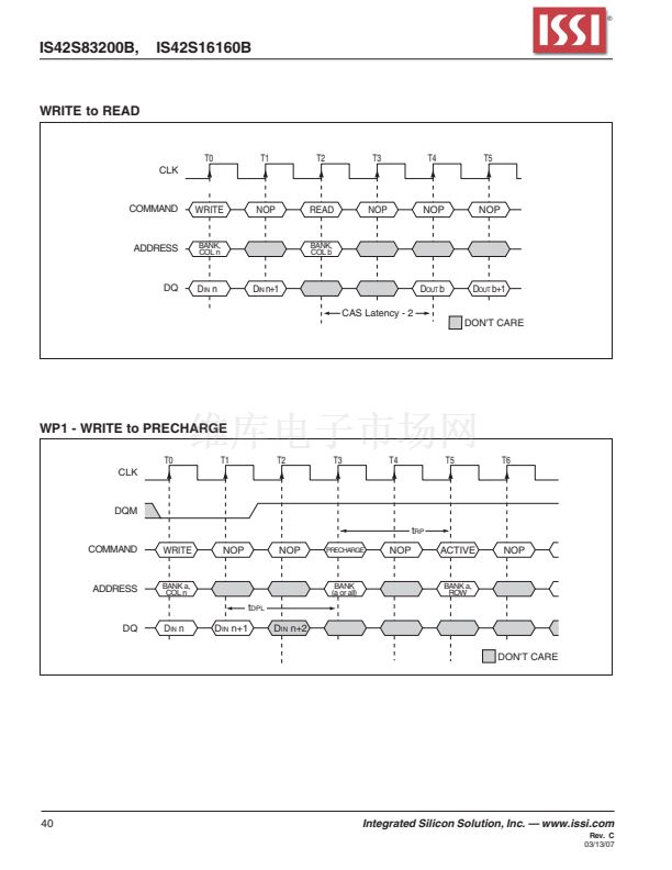
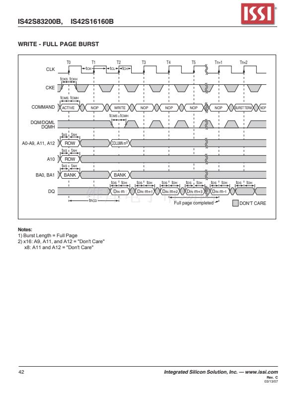
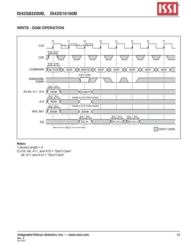
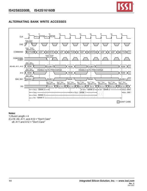
IS42S83200B,
PIN FUNCTIONS
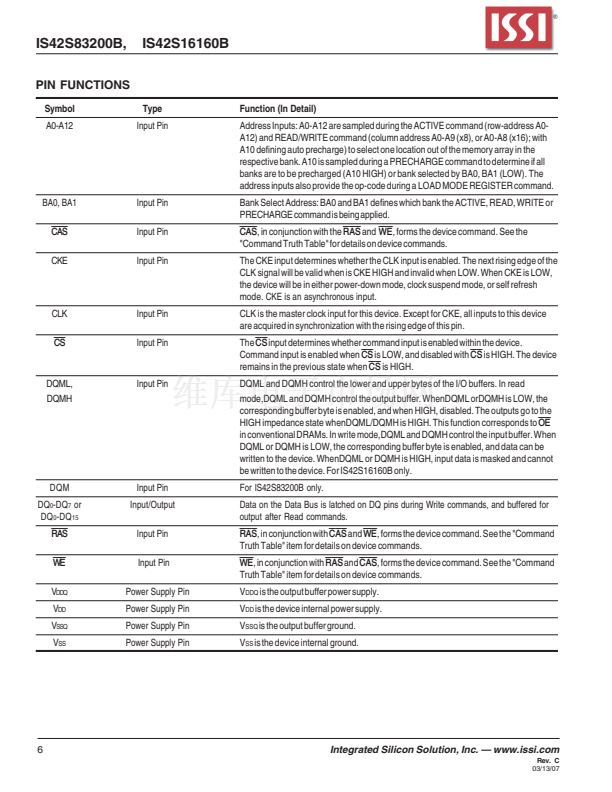
Symbol
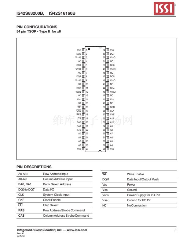
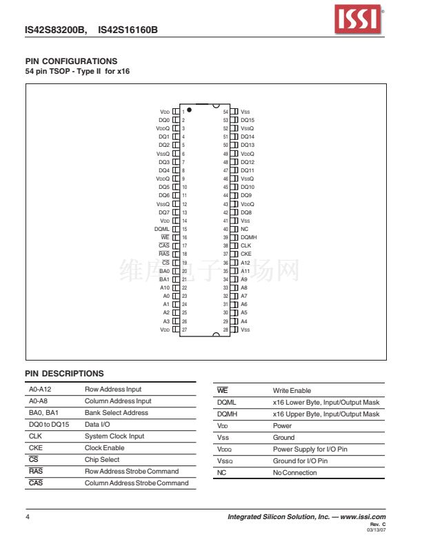
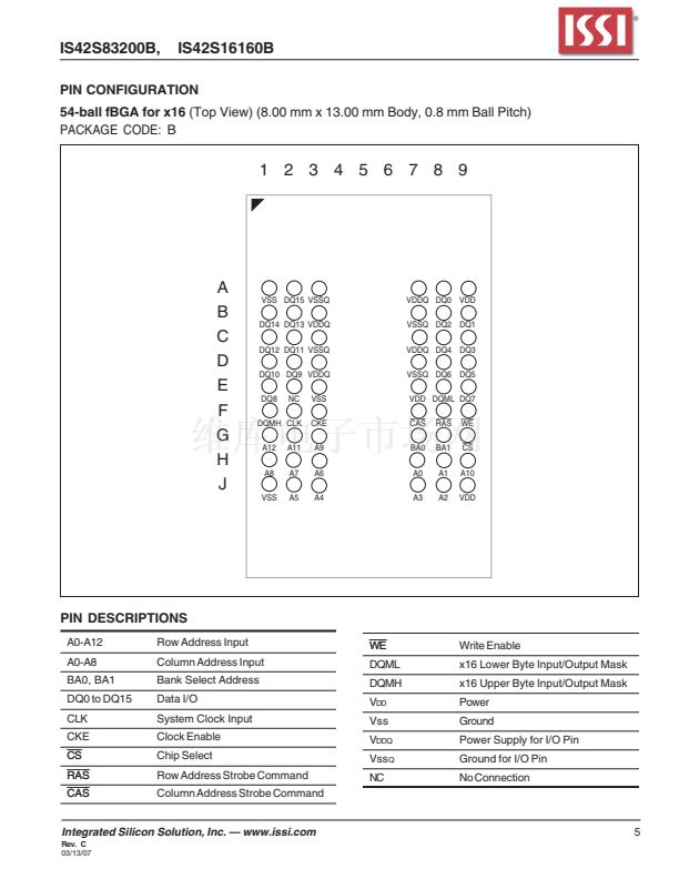
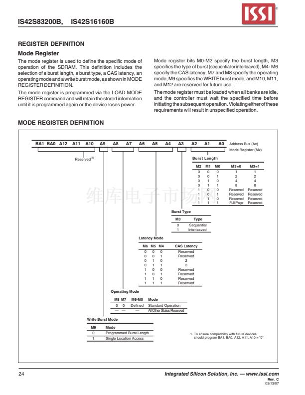
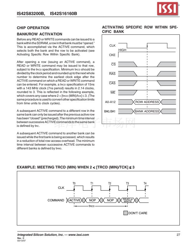
A0-A12
IS42S16160B
Type
Input Pin
Function (In Detail)
Address Inputs: A0-A12 are sampled during the ACTIVE command (row-address A0-
A12) and READ/WRITE command (column address A0-A9 (x8), or A0-A8 (x16); with
A10 defining auto precharge) to select one location out of the memory array in the
respective bank. A10 is sampled during a PRECHARGE command to determine if all
banks are to be precharged (A10 HIGH) or bank selected by BA0, BA1 (LOW). The
address inputs also provide the op-code during a LOAD MODE REGISTER command.
Bank Select Address: BA0 and BA1 defines which bank the ACTIVE, READ, WRITE or
PRECHARGE command is being applied.
CAS,
in conjunction with the
RAS
and
WE,
forms the device command. See the
"Command Truth Table" for details on device commands.
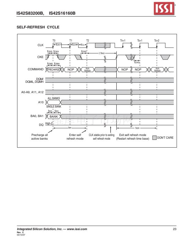
The CKE input determines whether the CLK input is enabled. The next rising edge of the
CLK signal will be valid when is CKE HIGH and invalid when LOW. When CKE is LOW,
the device will be in either power-down mode, clock suspend mode, or self refresh
mode. CKE is an asynchronous input.
CLK is the master clock input for this device. Except for CKE, all inputs to this device
are acquired in synchronization with the rising edge of this pin.
The
CS
input determines whether command input is enabled within the device.
Command input is enabled when
CS
is LOW, and disabled with
CS
is HIGH. The device
remains in the previous state when
CS
is HIGH.
DQML and DQMH control the lower and upper bytes of the I/O buffers. In read
mode,DQML and DQMH control the output buffer. WhenDQML orDQMH is LOW, the
corresponding buffer byte is enabled, and when HIGH, disabled. The outputs go to the
HIGH impedance state whenDQML/DQMH is HIGH. This function corresponds to
OE
in conventional DRAMs. In write mode,DQML and DQMH control the input buffer. When
DQML or DQMH is LOW, the corresponding buffer byte is enabled, and data can be
written to the device. WhenDQML or DQMH is HIGH, input data is masked and cannot
be written to the device. For IS42S16160B only.
For IS42S83200B only.
Data on the Data Bus is latched on DQ pins during Write commands, and buffered for
output after Read commands.
RAS,
in conjunction with
CAS
and
WE,
forms the device command. See the "Command
Truth Table" item for details on device commands.
WE,
in conjunction with
RAS
and
CAS,
forms the device command. See the "Command
Truth Table" item for details on device commands.
V
DDQ
is the output buffer power supply.
V
DD
is the device internal power supply.
V
SSQ
is the output buffer ground.
V
SS
is the device internal ground.
BA0, BA1
CAS
CKE
Input Pin
Input Pin
Input Pin
CLK
CS
Input Pin
Input Pin
DQML,
DQMH
Input Pin
DQM
DQ
0
-DQ
7
or
DQ
0
-DQ
15
RAS
WE
V
DDQ
V
DD
V
SSQ
V
SS
Input Pin
Input/Output
Input Pin
Input Pin
Power Supply Pin
Power Supply Pin
Power Supply Pin
Power Supply Pin
6
Integrated Silicon Solution, Inc. 鈥?www.issi.com
Rev. C
03/13/07


 1
1
 2
2
 3
3
 4
4
 5
5
 6
6
 7
7
 8
8
 9
9
 10
10
 11
11
 12
12
 13
13
 14
14
 15
15
 16
16
 17
17
 18
18
 19
19
 20
20
 21
21
 22
22
 23
23
 24
24
 25
25
 26
26
 27
27
 28
28
 29
29
 30
30
 31
31
 32
32
 33
33
 34
34
 35
35
 36
36
 37
37
 38
38
 39
39
 40
40
 41
41
 42
42
 43
43
 44
44
 45
45
 46
46
 47
47
 48
48
 49
49
 50
50
 51
51
 52
52
 53
53
 54
54
 55
55
 56
56
 57
57
 58
58
 59
59
 60
60
 61
61
 62
62
 63
63
