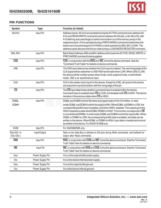
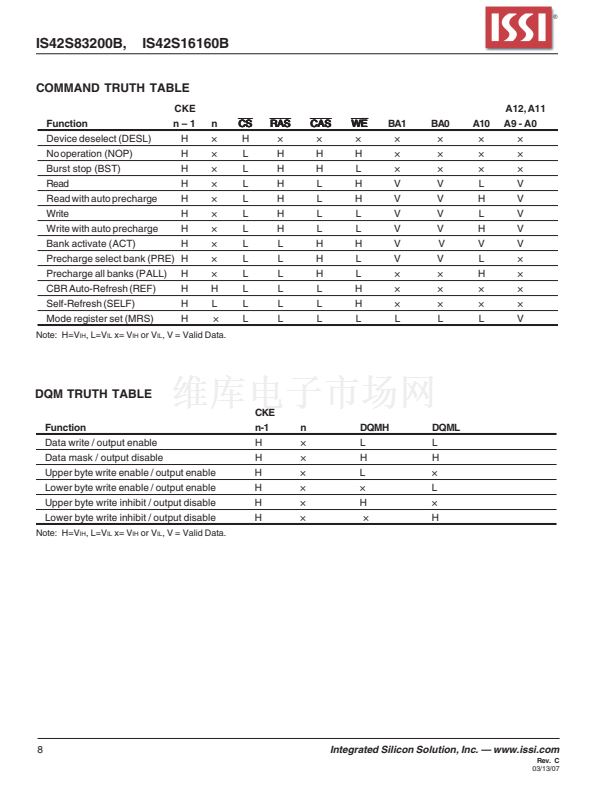
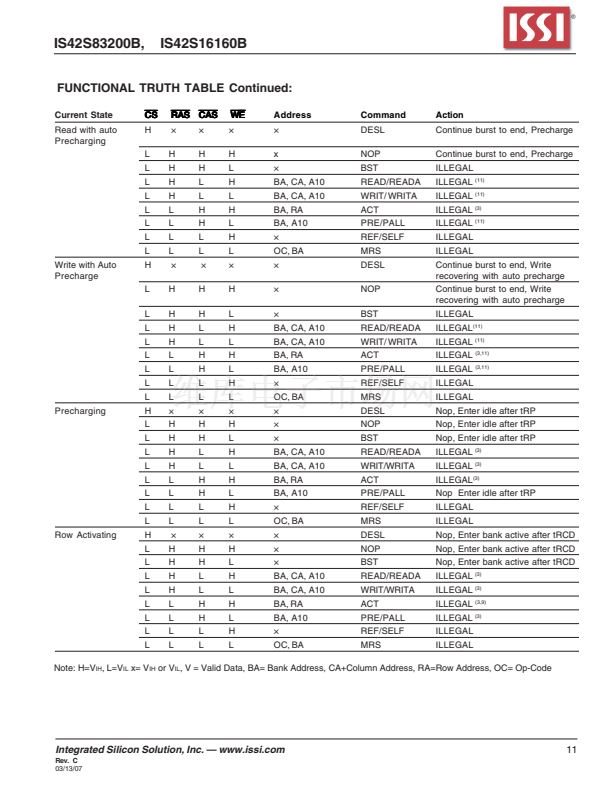
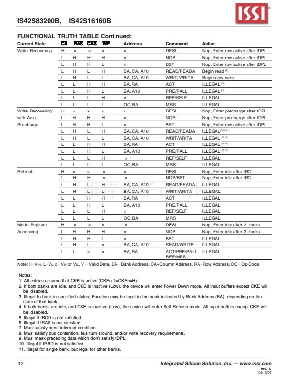
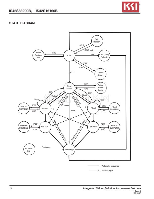
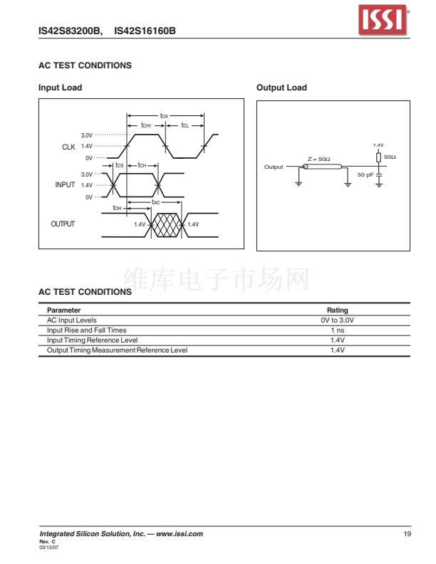
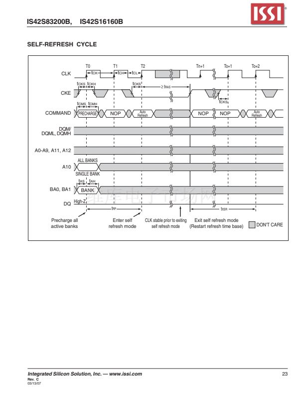
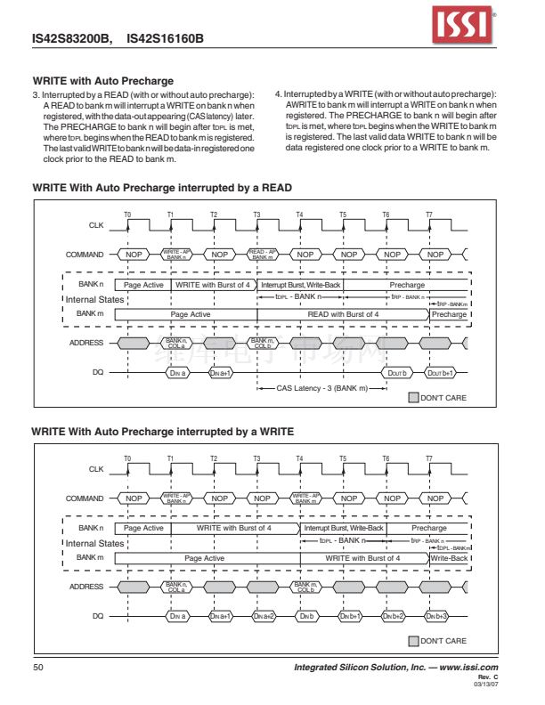
IS42S83200B,
READS
IS42S16160B
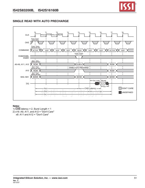
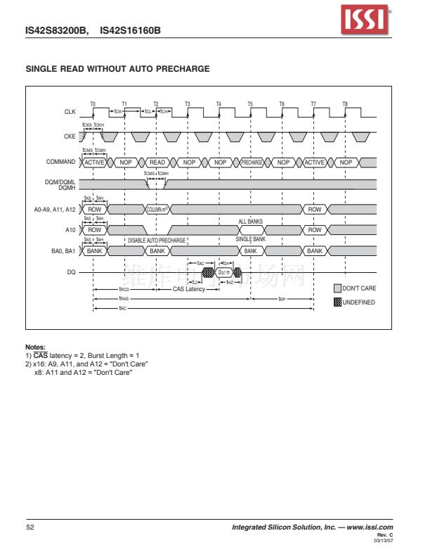
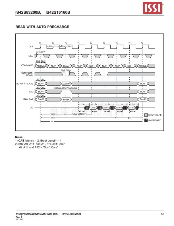
READ COMMAND
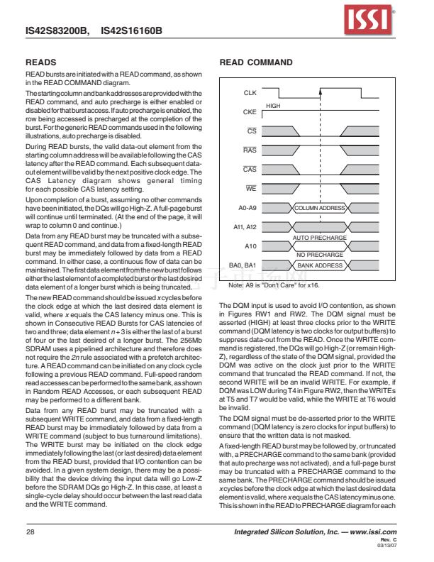
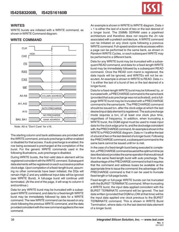
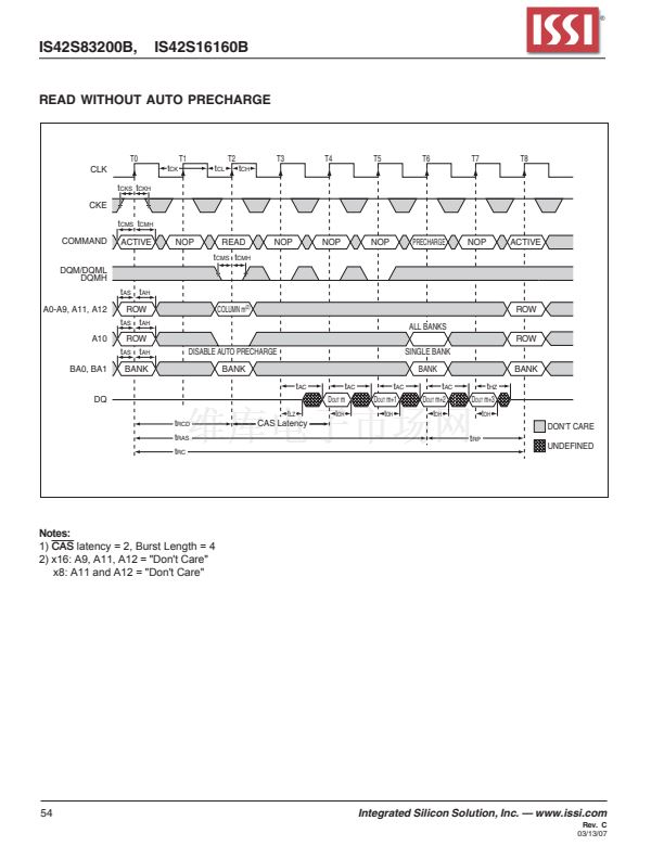
READ bursts are initiated with a READ command, as shown
in the READ COMMAND diagram.
The starting column and bank addresses are provided with the
READ command, and auto precharge is either enabled or
disabled for that burst access. If auto precharge is enabled, the
row being accessed is precharged at the completion of the
burst. For the generic READ commands used in the following
illustrations, auto precharge is disabled.
During READ bursts, the valid data-out element from the
starting column address will be available following the CAS
latency after the READ command. Each subsequent data-
out element will be valid by the next positive clock edge. The
CAS Latency diagram shows general timing
for each possible CAS latency setting.
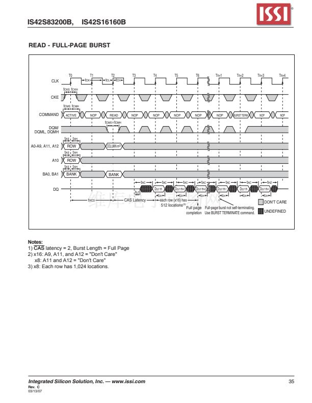
Upon completion of a burst, assuming no other commands
have been initiated, the DQs will go High-Z. A full-page burst
will continue until terminated. (At the end of the page, it will
wrap to column 0 and continue.)
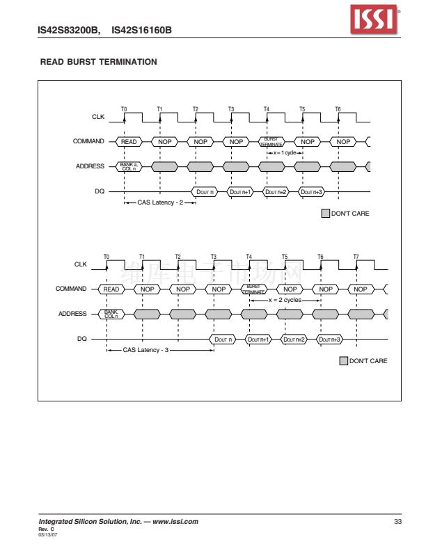
Data from any READ burst may be truncated with a subse-
quent READ command, and data from a fixed-length READ
burst may be immediately followed by data from a READ
command. In either case, a continuous flow of data can be
maintained. The first data element from the new burst follows
either the last element of a completed burst or the last desired
data element of a longer burst which is being truncated.
The new READ command should be issued
x
cycles before
the clock edge at which the last desired data element is
valid, where
x
equals the CAS latency minus one. This is
shown in Consecutive READ Bursts for CAS latencies of
two and three; data element
n
+ 3 is either the last of a burst
of four or the last desired of a longer burst. The 256Mb
SDRAM uses a pipelined architecture and therefore does
not require the
2n
rule associated with a prefetch architec-
ture. A READ command can be initiated on any clock cycle
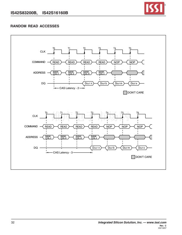
following a previous READ command. Full-speed random
read accesses can be performed to the same bank, as shown
in Random READ Accesses, or each subsequent READ
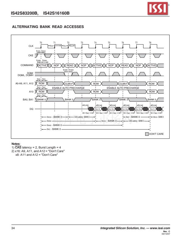
may be performed to a different bank.
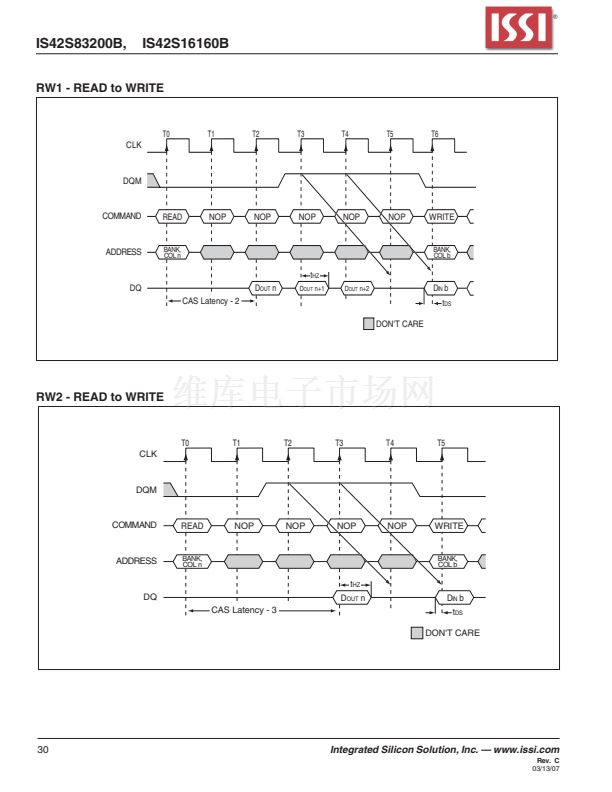
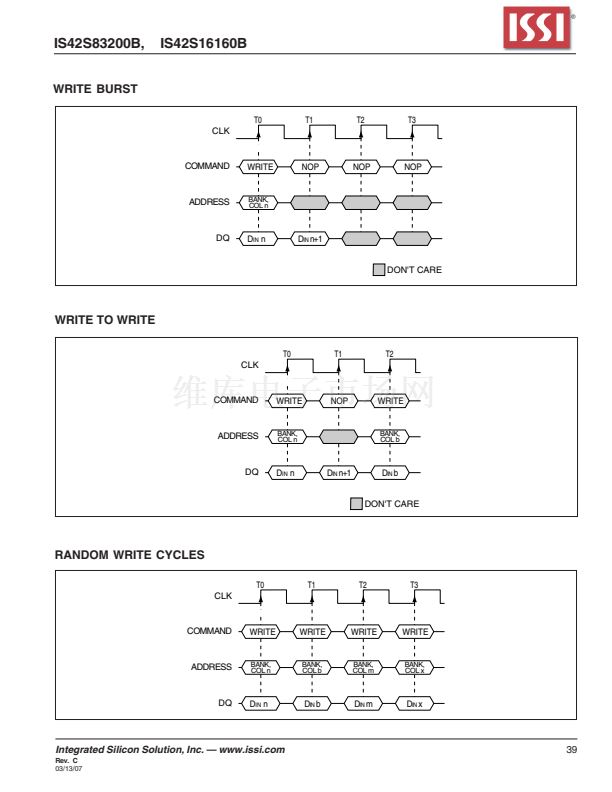
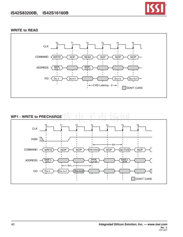
Data from any READ burst may be truncated with a
subsequent WRITE command, and data from a fixed-length
READ burst may be immediately followed by data from a
WRITE command (subject to bus turnaround limitations).
The WRITE burst may be initiated on the clock edge
immediately following the last (or last desired) data element
from the READ burst, provided that I/O contention can be
avoided. In a given system design, there may be a possi-
bility that the device driving the input data will go Low-Z
before the SDRAM DQs go High-Z. In this case, at least a
single-cycle delay should occur between the last read data
and the WRITE command.
CLK
HIGH
CKE
CS
RAS
CAS
WE
A0-A9
A11, A12
AUTO PRECHARGE
COLUMN ADDRESS
A10
NO PRECHARGE
BA0, BA1
BANK ADDRESS
Note: A9 is "Don't Care" for x16.
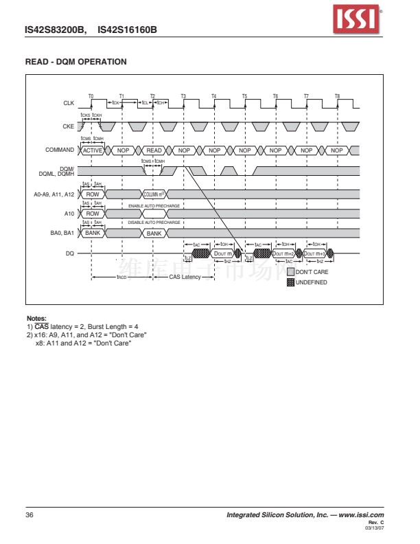
The DQM input is used to avoid I/O contention, as shown
in Figures RW1 and RW2. The DQM signal must be
asserted (HIGH) at least three clocks prior to the WRITE
command (DQM latency is two clocks for output buffers) to
suppress data-out from the READ. Once the WRITE com-
mand is registered, the DQs will go High-Z (or remain High-
Z), regardless of the state of the DQM signal, provided the
DQM was active on the clock just prior to the WRITE
command that truncated the READ command. If not, the
second WRITE will be an invalid WRITE. For example, if
DQM was LOW during T4 in Figure RW2, then the WRITEs
at T5 and T7 would be valid, while the WRITE at T6 would
be invalid.
The DQM signal must be de-asserted prior to the WRITE
command (DQM latency is zero clocks for input buffers) to
ensure that the written data is not masked.
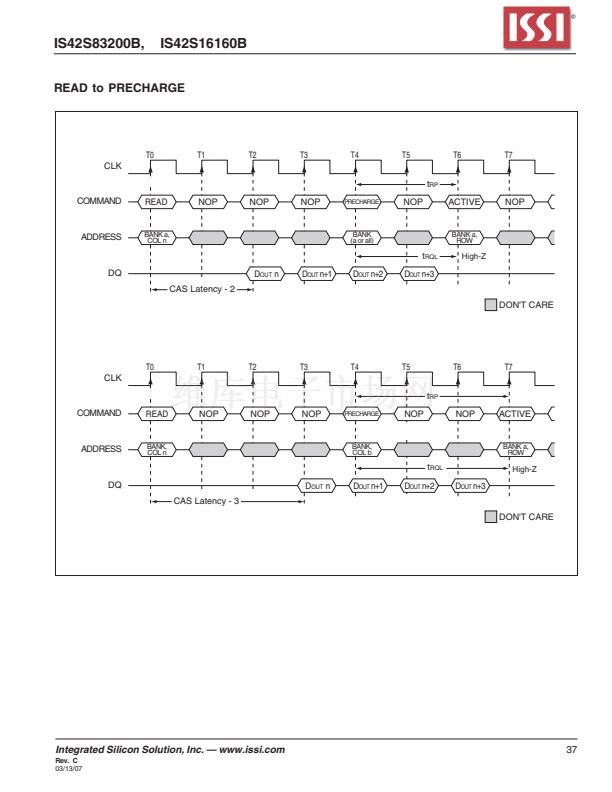
A fixed-length READ burst may be followed by, or truncated
with, a PRECHARGE command to the same bank (provided
that auto precharge was not activated), and a full-page burst
may be truncated with a PRECHARGE command to the
same bank. The PRECHARGE command should be issued
x
cycles before the clock edge at which the last desired data
element is valid, where
x
equals the CAS latency minus one.
This is shown in the READ to PRECHARGE diagram for each
28
Integrated Silicon Solution, Inc. 鈥?www.issi.com
Rev. C
03/13/07


 1
1
 2
2
 3
3
 4
4
 5
5
 6
6
 7
7
 8
8
 9
9
 10
10
 11
11
 12
12
 13
13
 14
14
 15
15
 16
16
 17
17
 18
18
 19
19
 20
20
 21
21
 22
22
 23
23
 24
24
 25
25
 26
26
 27
27
 28
28
 29
29
 30
30
 31
31
 32
32
 33
33
 34
34
 35
35
 36
36
 37
37
 38
38
 39
39
 40
40
 41
41
 42
42
 43
43
 44
44
 45
45
 46
46
 47
47
 48
48
 49
49
 50
50
 51
51
 52
52
 53
53
 54
54
 55
55
 56
56
 57
57
 58
58
 59
59
 60
60
 61
61
 62
62
 63
63
