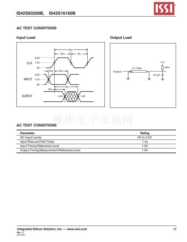
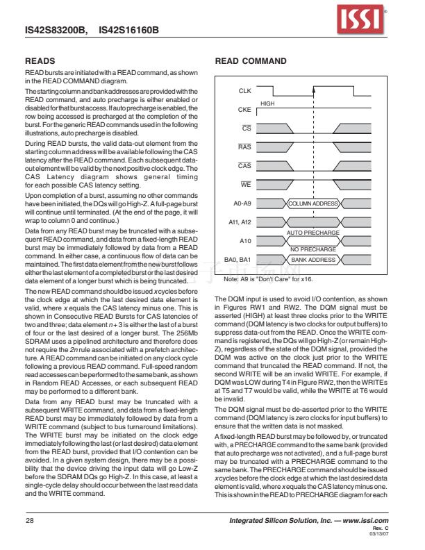
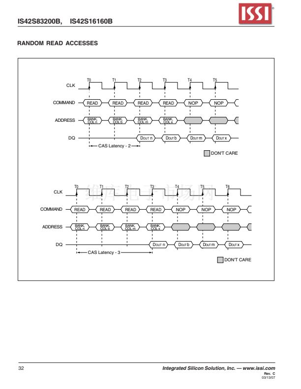
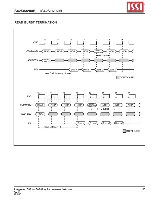
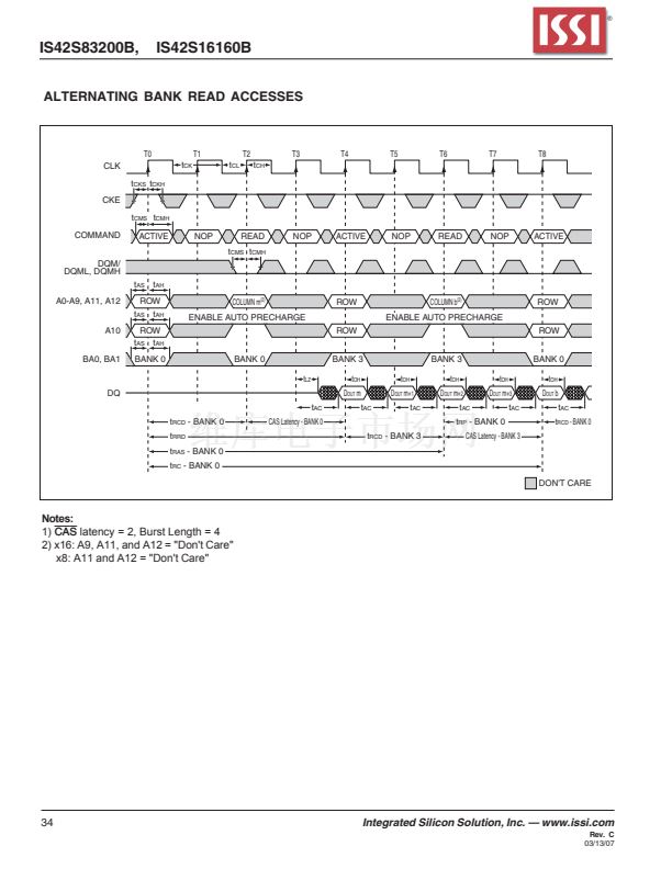
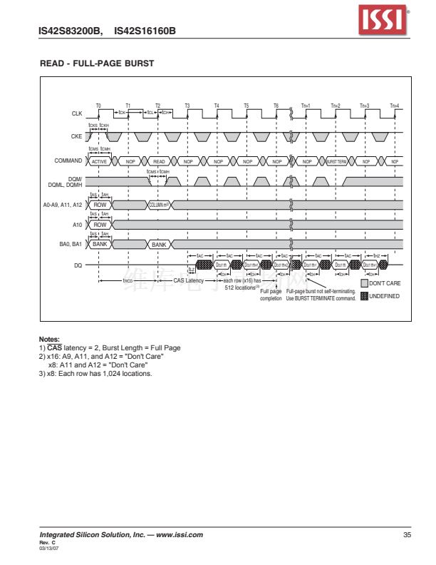
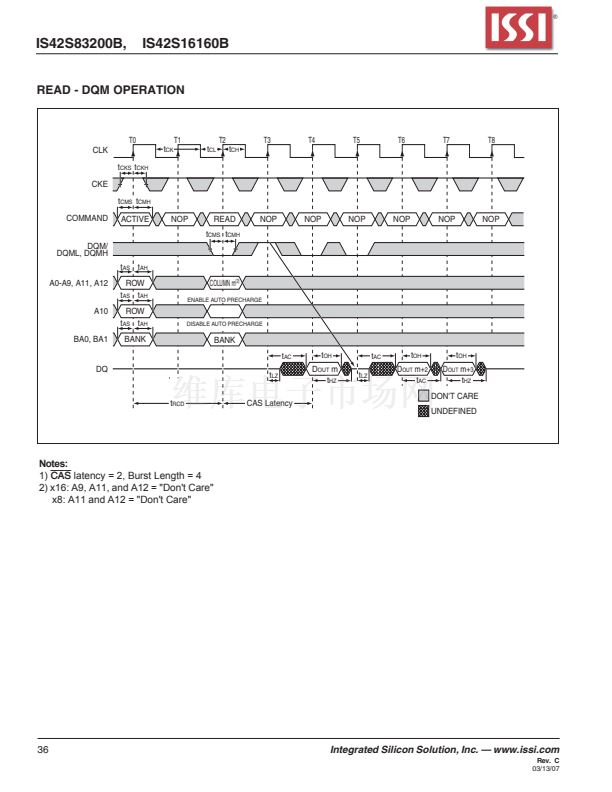
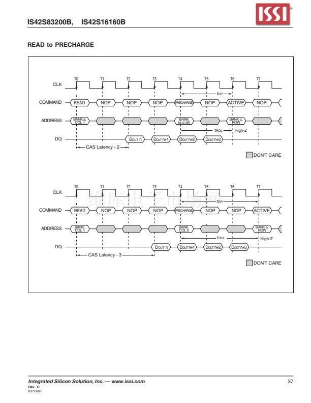
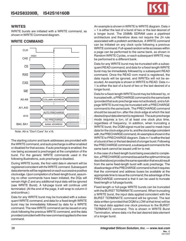
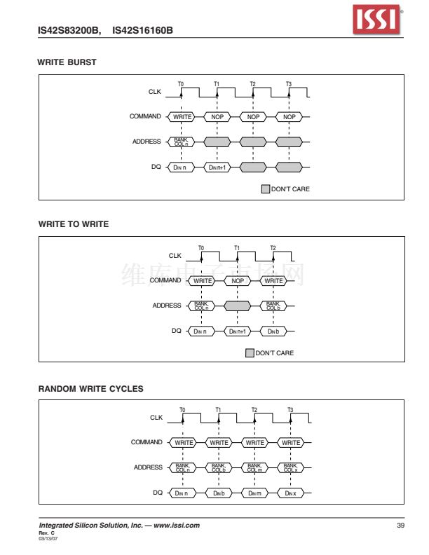
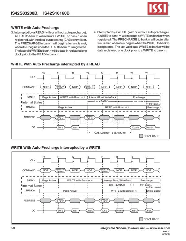
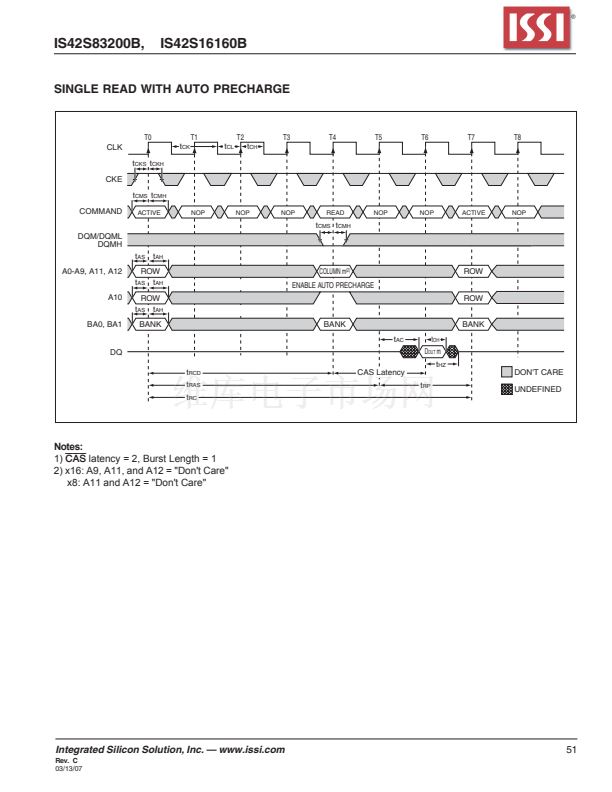
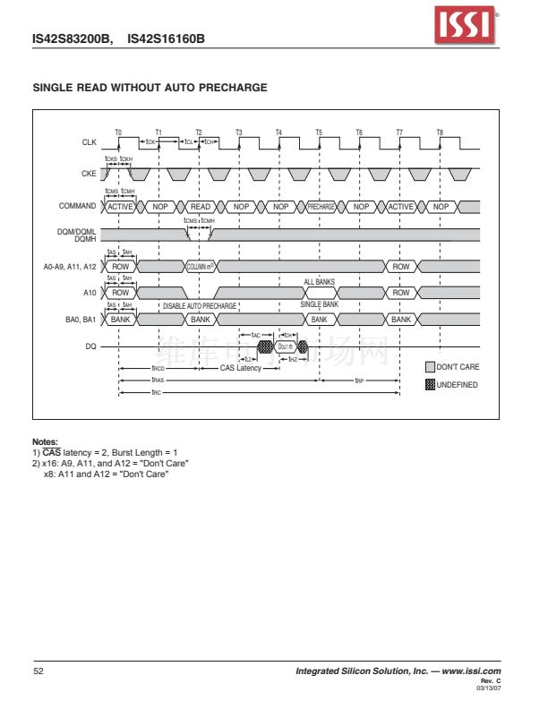
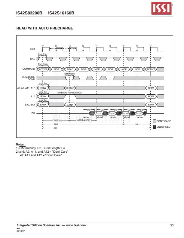
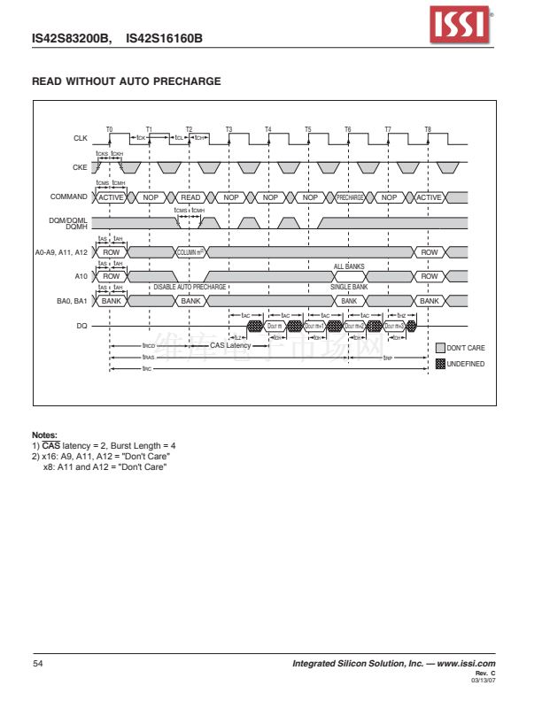
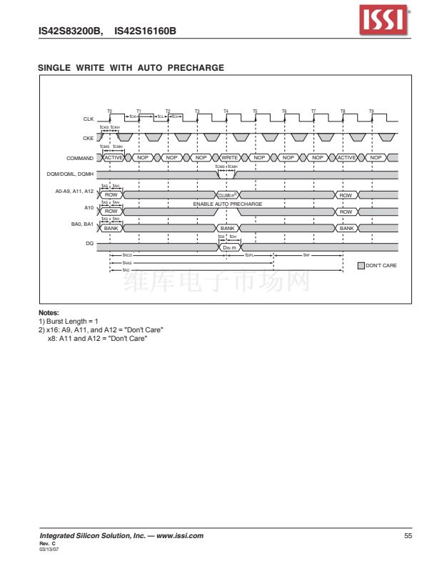
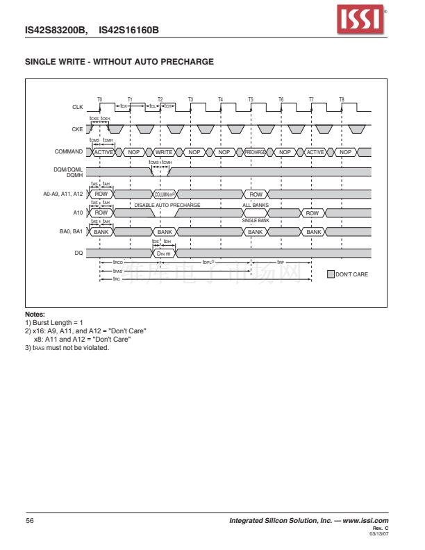
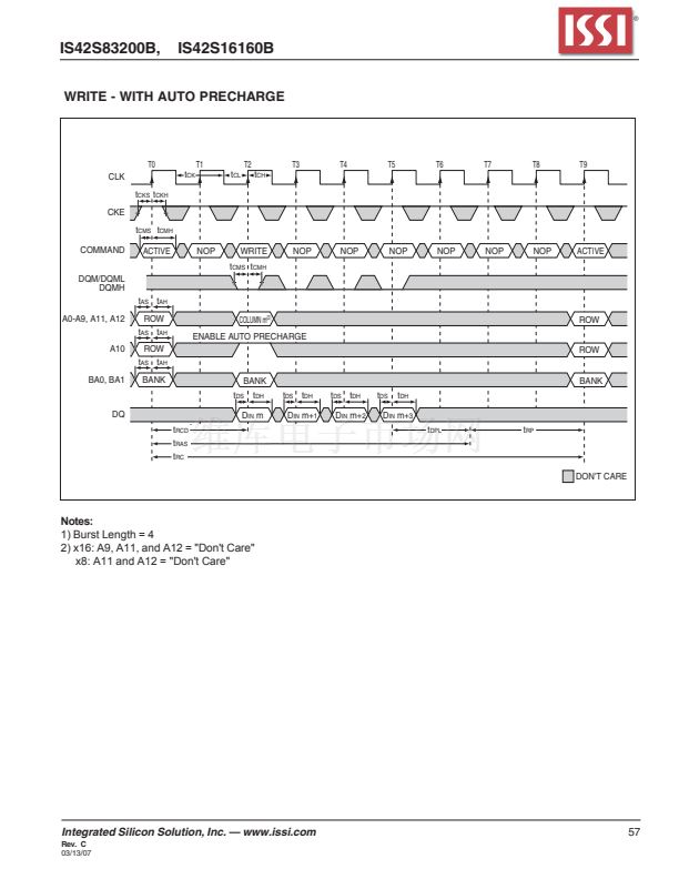
IS42S83200B,
IS42S16160B
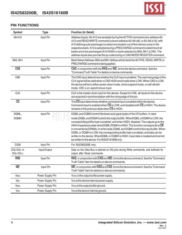
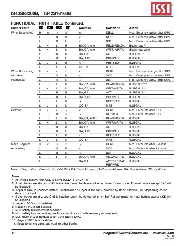
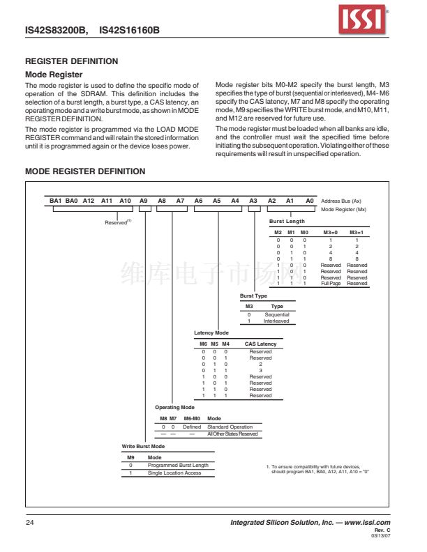
REGISTER DEFINITION
Mode Register
The mode register is used to define the specific mode of
operation of the SDRAM. This definition includes the
selection of a burst length, a burst type, a CAS latency, an
operating mode and a write burst mode, as shown in MODE
REGISTER DEFINITION.
The mode register is programmed via the LOAD MODE
REGISTER command and will retain the stored information
until it is programmed again or the device loses power.
Mode register bits M0-M2 specify the burst length, M3
specifies the type of burst (sequential or interleaved), M4- M6
specify the CAS latency, M7 and M8 specify the operating
mode, M9 specifies the WRITE burst mode, and M10, M11,
and M12 are reserved for future use.
The mode register must be loaded when all banks are idle,
and the controller must wait the specified time before
initiating the subsequent operation. Violating either of these
requirements will result in unspecified operation.
MODE REGISTER DEFINITION
BA1 BA0 A12
A11
A10
(1)
A9
A8
A7
A6
A5
A4
A3
A2
A1
A0
Address Bus (Ax)
Mode Register (Mx)
Reserved
Burst Length
M2
0
0
0
0
1
1
1
1
Burst Type
M3
0
1
Latency Mode
M6 M5 M4
0
0
0
0
1
1
1
1
Operating Mode
M8 M7
0 0
鈥?鈥?/div>
M6-M0
Defined
鈥?/div>
Mode
Standard Operation
All Other States Reserved
0
0
1
1
0
0
1
1
0
1
0
1
0
1
0
1
CAS Latency
Reserved
Reserved
2
3
Reserved
Reserved
Reserved
Reserved
Type
Sequential
Interleaved
M1
0
0
1
1
0
0
1
1
M0
0
1
0
1
0
1
0
1
M3=0
1
2
4
8
Reserved
Reserved
Reserved
Full Page
M3=1
1
2
4
8
Reserved
Reserved
Reserved
Reserved
Write Burst Mode
M9
0
1
Mode
Programmed Burst Length
Single Location Access
1. To ensure compatibility with future devices,
should program BA1, BA0, A12, A11, A10 = "0"
24
Integrated Silicon Solution, Inc. 鈥?www.issi.com
Rev. C
03/13/07


 1
1
 2
2
 3
3
 4
4
 5
5
 6
6
 7
7
 8
8
 9
9
 10
10
 11
11
 12
12
 13
13
 14
14
 15
15
 16
16
 17
17
 18
18
 19
19
 20
20
 21
21
 22
22
 23
23
 24
24
 25
25
 26
26
 27
27
 28
28
 29
29
 30
30
 31
31
 32
32
 33
33
 34
34
 35
35
 36
36
 37
37
 38
38
 39
39
 40
40
 41
41
 42
42
 43
43
 44
44
 45
45
 46
46
 47
47
 48
48
 49
49
 50
50
 51
51
 52
52
 53
53
 54
54
 55
55
 56
56
 57
57
 58
58
 59
59
 60
60
 61
61
 62
62
 63
63
