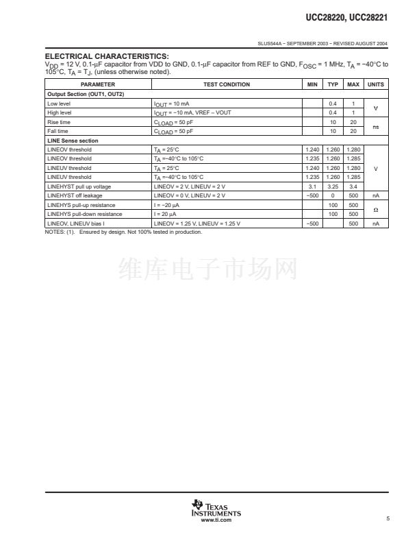
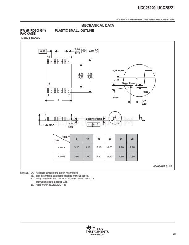
UCC28220, UCC28221
SLUS544A 鈭?SEPTEMBER 2003 鈭?REVISED AUGUST 2004
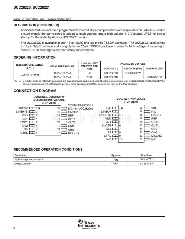
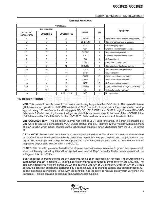
CHG:
A resistor from this pin to GND sets up the charging current of the internal C
T
capacitor used in the
oscillator. This resistor, in conjunction with the resistor on the DISCHG pin is used to set up the operating
frequency and maximum duty cycle. Under normal operation the dc voltage on this pin is 2.5 V.
DISCHG:
A resistor from this pin to GND sets up the discharge current of the internal C
T
capacitor used in the
oscillator. This resistor, in conjunction with the resistor on the CHG pin is used to set up the operating frequency
and maximum duty cycle. Under normal operation the dc voltage on this pin is 2.5 V.
OUT1 and OUT2:
These output buffers are intended to interface with high current MOSFET drivers. The output
drive capability is approximately 33 mA and has an output impedance of 100
鈩?
The outputs swing between
GND and REF.
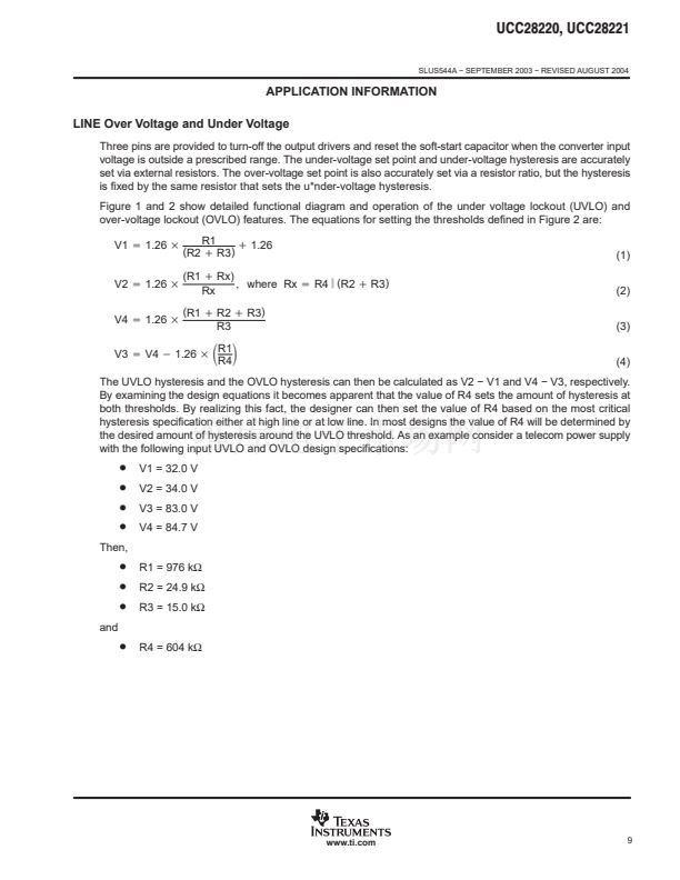
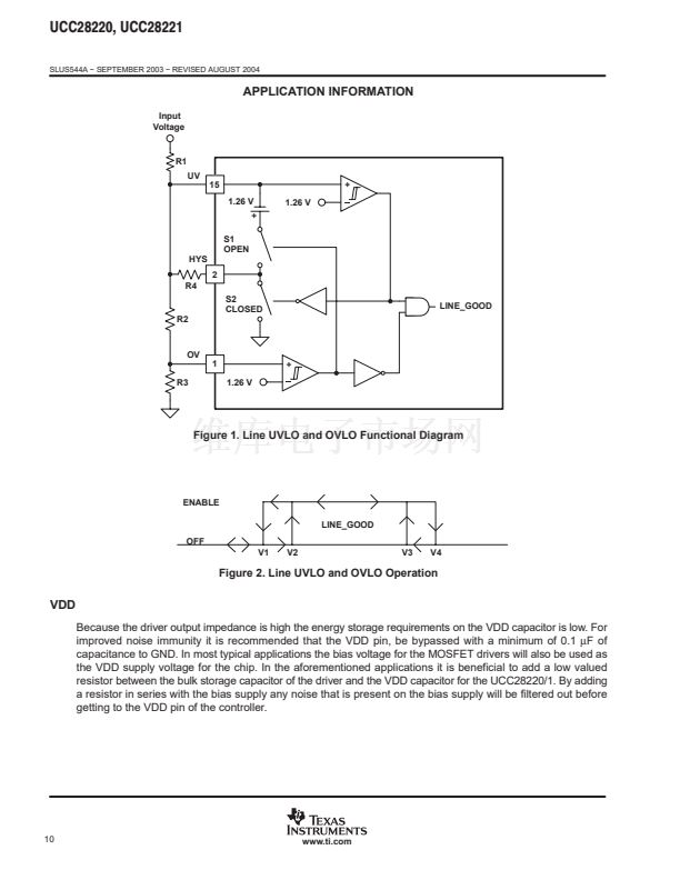
LINEOV:
This pin is connected to a comparator and used to monitor the line voltage for an over voltage
condition. The typical threshold is 1.26 V.
LINEUV:
This pin is connected to a comparator and used to monitor the line voltage for an under voltage
condition. The typical threshold is 1.26 V.
LINEHYST:
This pin is controlled by both the LINEOV and LINEUV pins. It is used to control the hysteresis
values for both the over and under voltage line detectors.
REF:
REF is a 3.3-V output used primarily as a source for the output buffers and other internal circuits. It is
protected from accidental shorts to ground. For improved noise immunity it is recommended that the reference
pin be bypassed with a minimum of 0.1
碌F
of capacitance to GND.
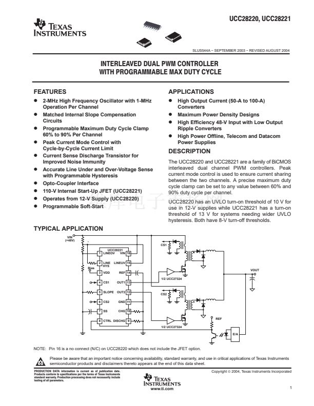
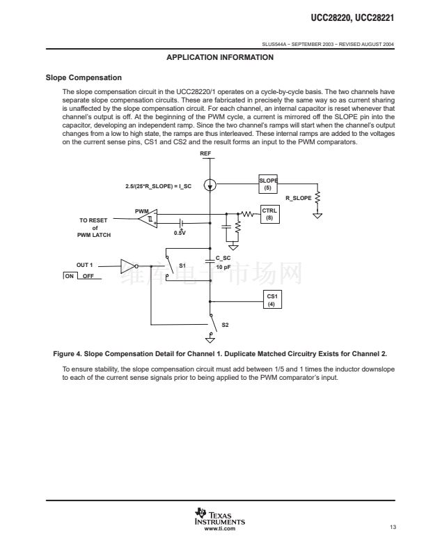
APPLICATION INFORMATION
General
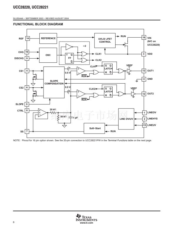
The device is comprised of several housekeeping blocks as well as two slope compensated PWM channels that
are interleaved. The circuit is intended to run from an external VDD supply voltage between 8 V and 14 V,
however, the UCC28221 has the addition of a high voltage startup JFET with control circuitry which can be used
for system startup. Other functions contained in the device are supply UVLO, 3.3-V reference, accurate line OV
and UV functions, a high speed programmable oscillator for both frequency and duty cycle, programmable slope
compensation, and programmable soft start functions.
The UCC28220/1 is a primary side controller for a two channel interleaved power converter. The device is
compatible with forward or flyback converters as long as a duty cycle clamp between 60 and 90 percent is
required. The active clamp forward and flyback converters as well as the RCD and resonant reset forward
converters are therefore compatible with this device. To ensure the two channels share the total converter output
current, current mode control with internal slope compensation is used. Slope compensation is user
programmable via a dedicated pin and can be set over a 50:1 range, ensuring good small-signal stability over
a wide range of applications.
8
www.ti.com


 1
1
 2
2
 3
3
 4
4
 5
5
 6
6
 7
7
 8
8
 9
9
 10
10
 11
11
 12
12
 13
13
 14
14
 15
15
 16
16
 17
17
 18
18
 19
19
 20
20
 21
21
 22
22
 23
23
 24
24
