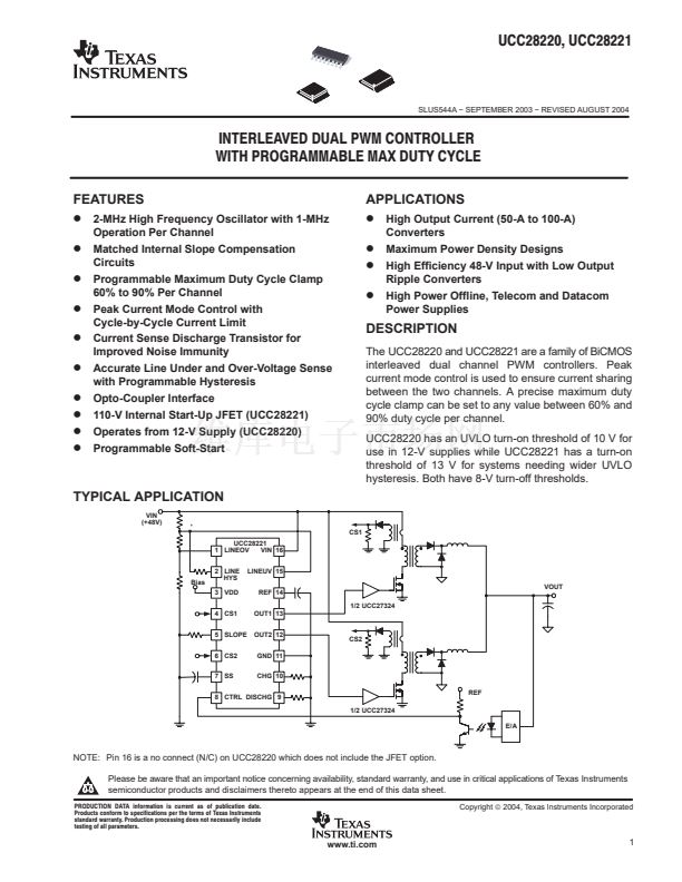
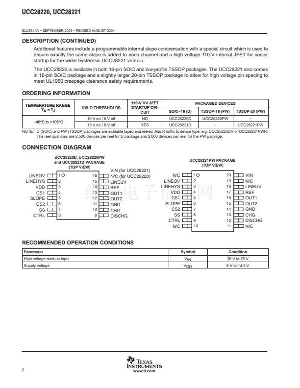
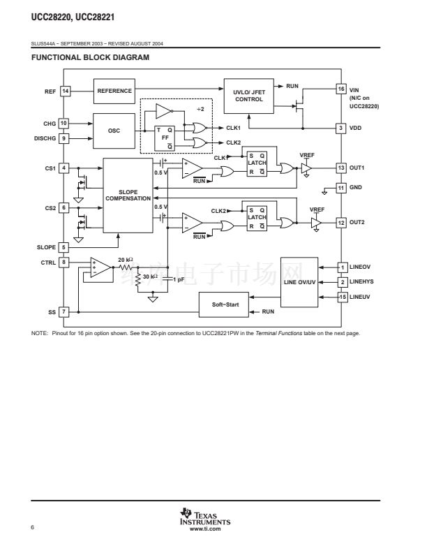
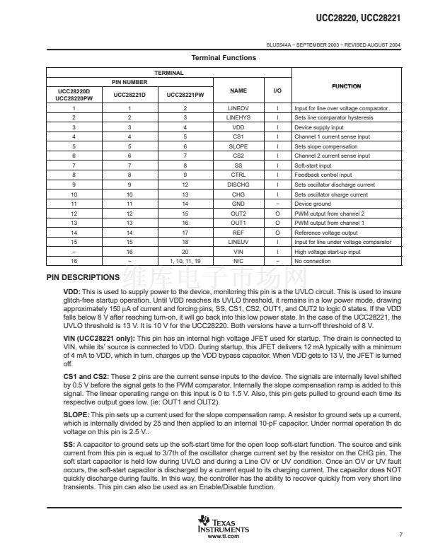
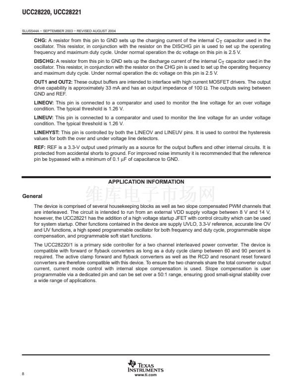
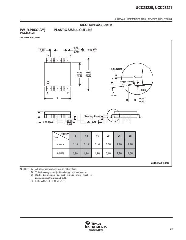
UCC28220, UCC28221
SLUS544A 鈭?SEPTEMBER 2003 鈭?REVISED AUGUST 2004
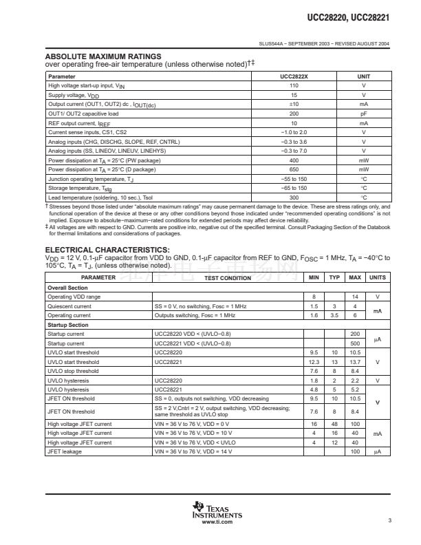
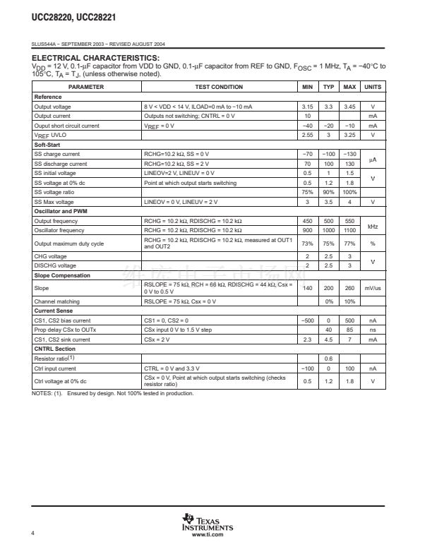
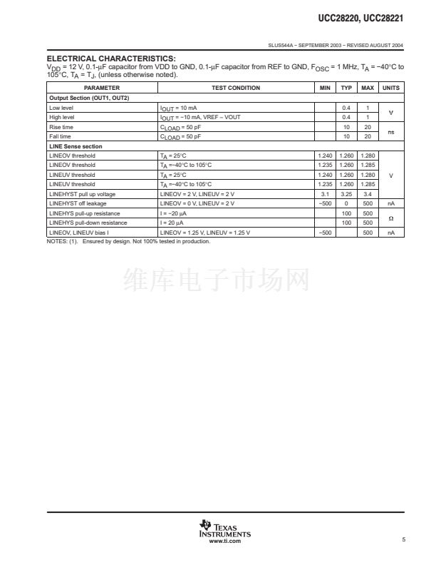
ELECTRICAL CHARACTERISTICS:
V
DD
= 12 V, 0.1-碌F capacitor from VDD to GND, 0.1-碌F capacitor from REF to GND, F
OSC
= 1 MHz, T
A
= 鈭?0擄C to
105擄C, T
A
= T
J
, (unless otherwise noted).
PARAMETER
Reference
Output voltage
Output current
Ouput short circuit current
VREF UVLO
Soft-Start
SS charge current
SS discharge current
SS initial voltage
SS voltage at 0% dc
SS voltage ratio
SS Max voltage
Oscillator and PWM
Output frequency
Oscillator frequency
Output maximum duty cycle
CHG voltage
DISCHG voltage
Slope Compensation
Slope
Channel matching
Current Sense
CS1, CS2 bias current
Prop delay CSx to OUTx
CS1, CS2 sink current
CNTRL Section
Resistor ratio(1)
Ctrl input current
Ctrl voltage at 0% dc
CTRL = 0 V and 3.3 V
CSx = 0 V, Point at which output starts switching (checks
resistor ratio)
鈭?00
0.5
CS1 = 0, CS2 = 0
CSx input 0 V to 1.5 V step
CSx = 2 V
2.3
鈭?00
0
40
4.5
0.6
0
1.2
100
1.8
nA
V
500
85
7
nA
ns
mA
RSLOPE = 75 k鈩? RCH = 66 k鈩? RDISCHG = 44 k鈩? Csx =
0 V to 0.5 V
RSLOPE = 75 k鈩? Csx = 0 V
140
200
0%
260
10%
mV/us
RCHG = 10.2 k鈩? RDISCHG = 10.2 k鈩?/div>
RCHG = 10.2 k鈩? RDISCHG = 10.2 k鈩?/div>
RCHG = 10.2 k鈩? RDISCHG = 10.2 k鈩? measured at OUT1
and OUT2
450
900
73%
2
2
500
1000
75%
2.5
2.5
550
1100
77%
3
3
V
kHz
%
LINEOV = 0 V, LINEUV = 2 V
RCHG=10.2 k鈩? SS = 0 V
RCHG=10.2 k鈩? SS = 2 V
LINEOV=2 V, LINEUV = 0 V
Point at which output starts switching
8 V < VDD < 14 V, ILOAD=0 mA to 鈭?0 mA
Outputs not switching; CNTRL = 0 V
VREF = 0 V
3.15
10
鈭?0
2.55
鈭?0
70
0.5
0.5
75%
3
鈭?0
3
鈭?00
100
1
1.2
90%
3.5
鈭?0
3.25
鈭?30
130
1.5
1.8
100%
4
V
V
3.3
3.45
V
mA
mA
V
TEST CONDITION
MIN
TYP
MAX
UNITS
碌A(chǔ)
A
NOTES: (1). Ensured by design. Not 100% tested in production.
4
www.ti.com


 1
1
 2
2
 3
3
 4
4
 5
5
 6
6
 7
7
 8
8
 9
9
 10
10
 11
11
 12
12
 13
13
 14
14
 15
15
 16
16
 17
17
 18
18
 19
19
 20
20
 21
21
 22
22
 23
23
 24
24
