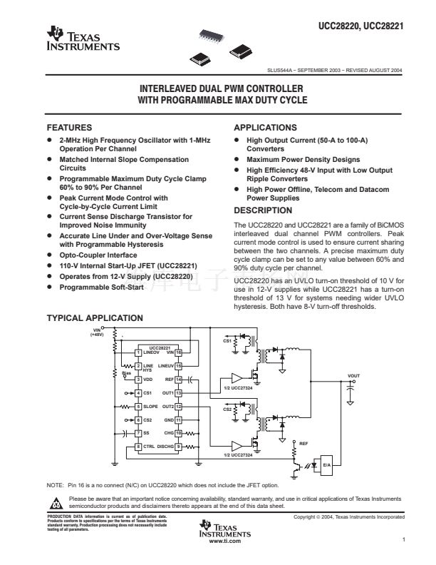
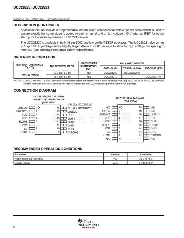
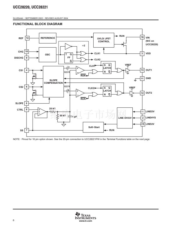
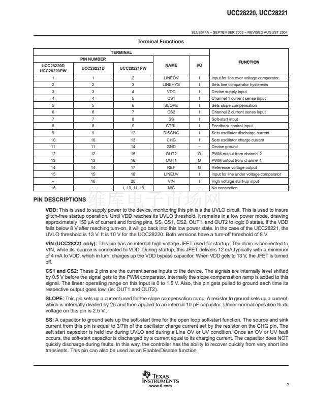
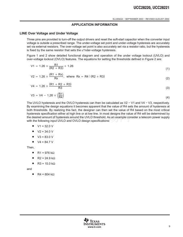
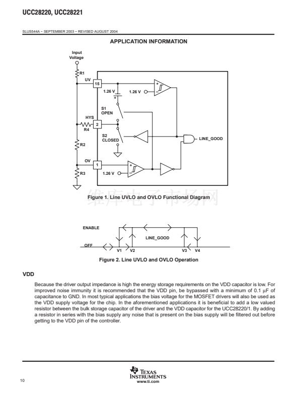
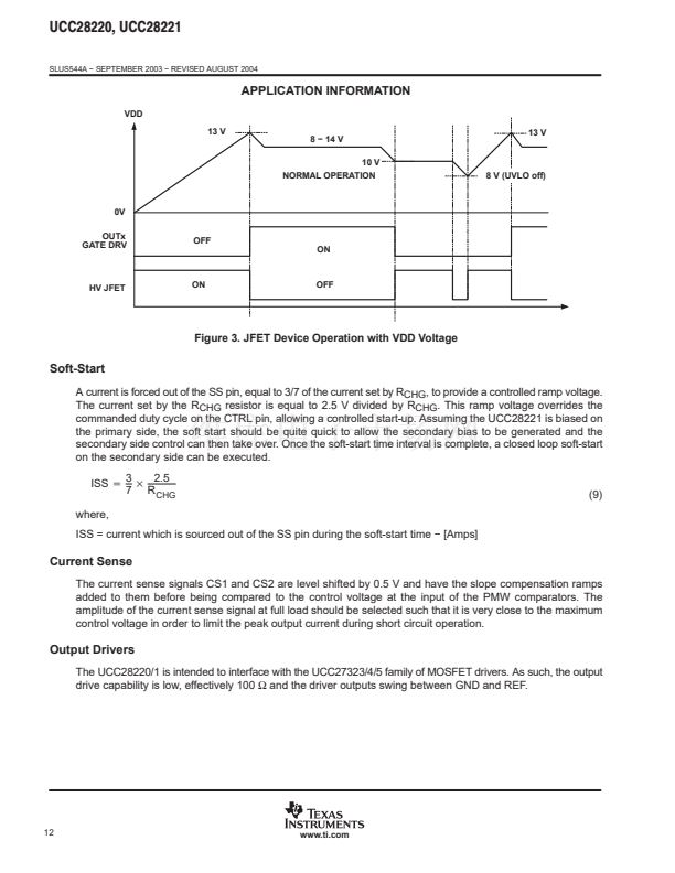
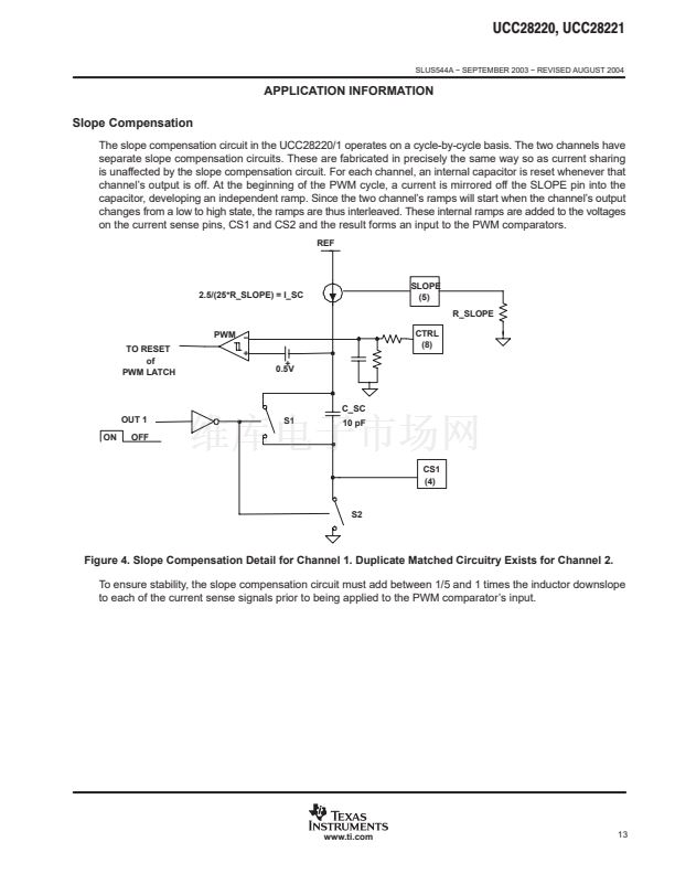
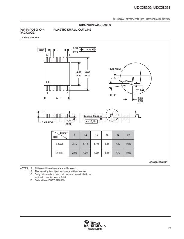
UCC28220, UCC28221
SLUS544A 鈭?SEPTEMBER 2003 鈭?REVISED AUGUST 2004
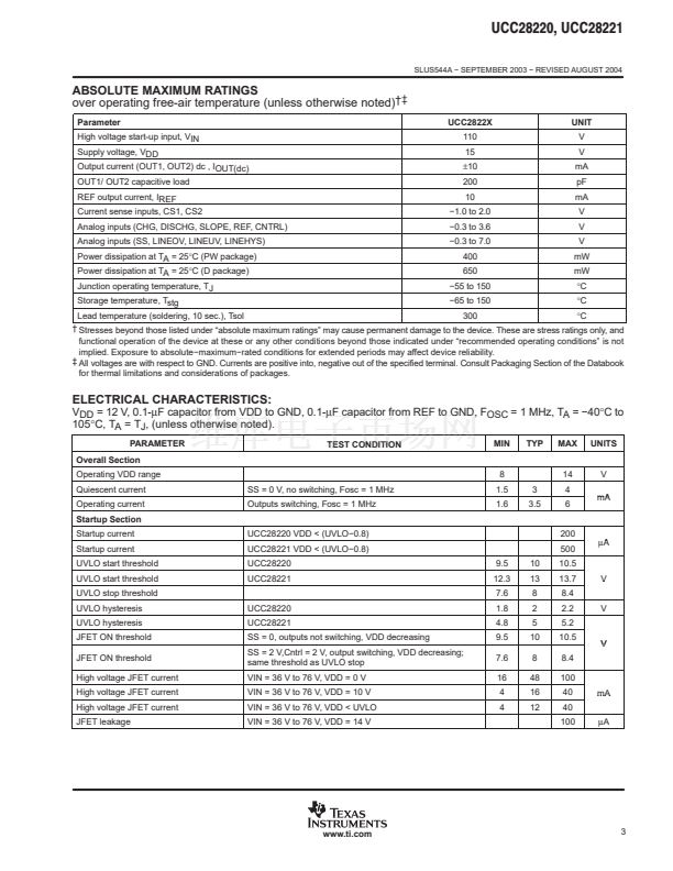
ABSOLUTE MAXIMUM RATINGS
over operating free-air temperature (unless otherwise noted)
鈥爙
Parameter
High voltage start-up input, VIN
Supply voltage, VDD
Output current (OUT1, OUT2) dc , IOUT(dc)
OUT1/ OUT2 capacitive load
REF output current, IREF
Current sense inputs, CS1, CS2
Analog inputs (CHG, DISCHG, SLOPE, REF, CNTRL)
Analog inputs (SS, LINEOV, LINEUV, LINEHYS)
Power dissipation at TA = 25擄C (PW package)
Power dissipation at TA = 25擄C (D package)
Junction operating temperature, TJ
Storage temperature, Tstg
Lead temperature (soldering, 10 sec.), Tsol
UCC2822X
110
15
鹵10
200
10
鈭?.0 to 2.0
鈭?.3 to 3.6
鈭?.3 to 7.0
400
650
鈭?5 to 150
鈭?5 to 150
300
UNIT
V
V
mA
pF
mA
V
V
V
mW
mW
擄C
擄C
擄C
鈥?Stresses beyond those listed under 鈥渁bsolute maximum ratings鈥?may cause permanent damage to the device. These are stress ratings only, and
functional operation of the device at these or any other conditions beyond those indicated under 鈥渞ecommended operating conditions鈥?is not
implied. Exposure to absolute鈭抦aximum鈭抮ated conditions for extended periods may affect device reliability.
鈥?All voltages are with respect to GND. Currents are positive into, negative out of the specified terminal. Consult Packaging Section of the Databook
for thermal limitations and considerations of packages.
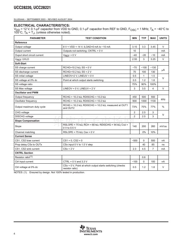
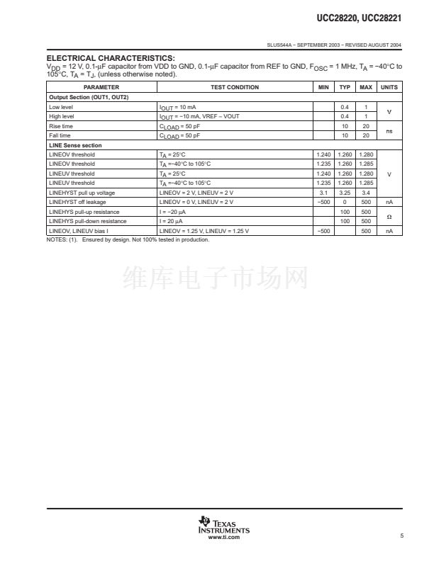
ELECTRICAL CHARACTERISTICS:
V
DD
= 12 V, 0.1-碌F capacitor from VDD to GND, 0.1-碌F capacitor from REF to GND, F
OSC
= 1 MHz, T
A
= 鈭?0擄C to
105擄C, T
A
= T
J
, (unless otherwise noted).
PARAMETER
Overall Section
Operating VDD range
Quiescent current
Operating current
Startup Section
Startup current
Startup current
UVLO start threshold
UVLO start threshold
UVLO stop threshold
UVLO hysteresis
UVLO hysteresis
JFET ON threshold
JFET ON threshold
High voltage JFET current
High voltage JFET current
High voltage JFET current
JFET leakage
UCC28220
UCC28221
SS = 0, outputs not switching, VDD decreasing
SS = 2 V,Cntrl = 2 V, output switching, VDD decreasing;
same threshold as UVLO stop
VIN = 36 V to 76 V, VDD = 0 V
VIN = 36 V to 76 V, VDD = 10 V
VIN = 36 V to 76 V, VDD < UVLO
VIN = 36 V to 76 V, VDD = 14 V
UCC28220 VDD < (UVLO鈭?.8)
UCC28221 VDD < (UVLO鈭?.8)
UCC28220
UCC28221
9.5
12.3
7.6
1.8
4.8
9.5
7.6
16
4
4
10
13
8
2
5
10
8
48
16
12
200
500
10.5
13.7
8.4
2.2
5.2
10.5
8.4
100
40
40
100
碌A(chǔ)
mA
V
V
V
A
碌A(chǔ)
SS = 0 V, no switching, Fosc = 1 MHz
Outputs switching, Fosc = 1 MHz
8
1.5
1.6
3
3.5
14
4
6
mA
V
TEST CONDITION
MIN
TYP
MAX
UNITS
www.ti.com
3


 1
1
 2
2
 3
3
 4
4
 5
5
 6
6
 7
7
 8
8
 9
9
 10
10
 11
11
 12
12
 13
13
 14
14
 15
15
 16
16
 17
17
 18
18
 19
19
 20
20
 21
21
 22
22
 23
23
 24
24
