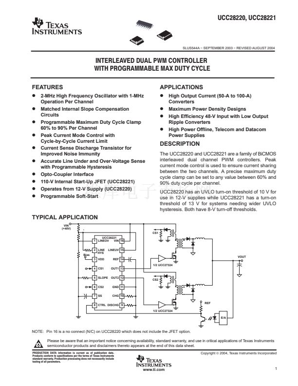
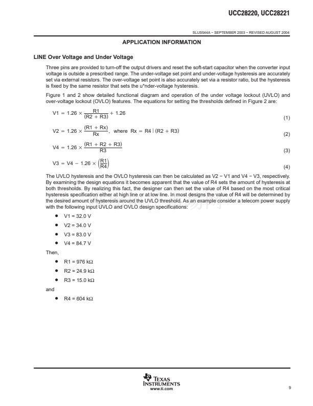
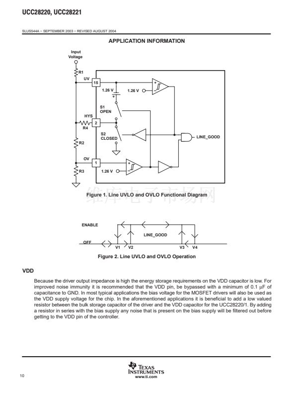
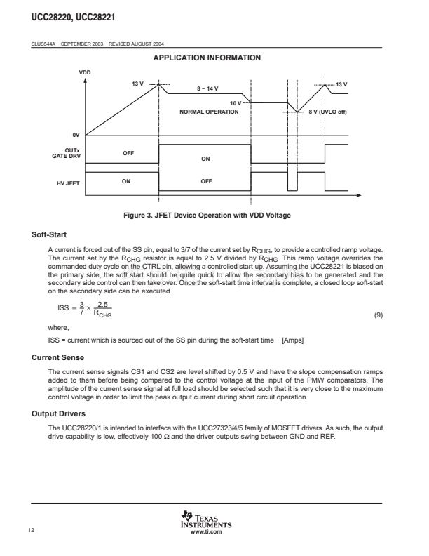
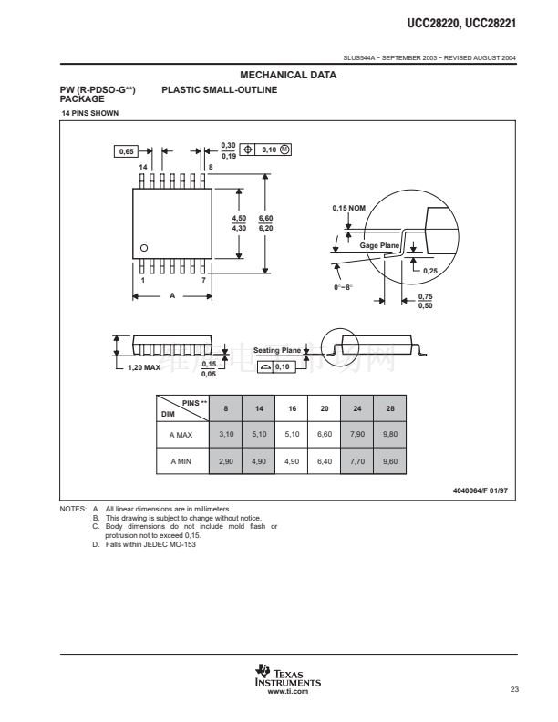
UCC28220, UCC28221
SLUS544A 鈭?SEPTEMBER 2003 鈭?REVISED AUGUST 2004
DESCRIPTION (CONTINUED)
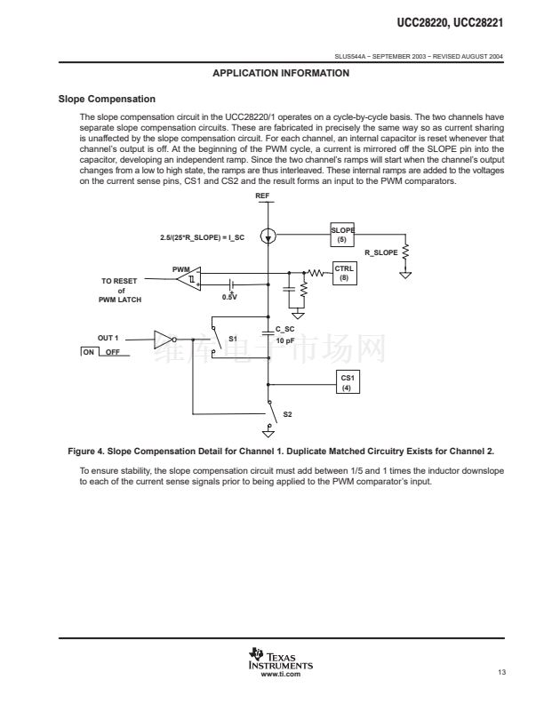
Additional features include a programmable internal slope compensation with a special circuit which is used to
ensure exactly the same slope is added to each channel and a high voltage 110-V internal JFET for easier
startup for the wider hysteresis UCC28221 version.
The UCC28220 is available in both 16-pin SOIC and low-profile TSSOP packages. The UCC28221 also comes
in 16-pin SOIC package and a slightly larger 20-pin TSSOP package to allow for high voltage pin spacing to
meet UL1950 creepage clearance safety requirements.
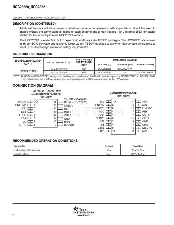
ORDERING INFORMATION
TEMPERATURE RANGE
TA = TJ
鈭?0擄C to +105擄C
UVLO THRESHOLDS
10 V on / 8 V off
13 V on / 8 V off
110-V HV JFET
STARTUP CIR-
CUIT
NO
YES
PACKAGED DEVICES
SOIC鈭?6 (D)
UCC28220D
UCC28221D
TSSOP-16 (PW)
UCC28220PW
鈭?/div>
TSSOP-20 (PW)
鈭?/div>
UCC28221PW
NOTE: D (SOIC) and PW (TSSOP) packages are available taped and reeled. Add R suffix to device type, e.g. UCC28220DR or UCC28221PWR.
The reel quanities are 2,500 devices per reel for D package and 2,000 devices per reel for the PW package.
CONNECTION DIAGRAM
UCC28220D, UCC28220PW
and UCC28221D PACKAGE
(TOP VIEW)
UCC28221PW PACKAGE
(TOP VIEW)
LINEOV
LINEHYS
VDD
CS1
SLOPE
CS2
SS
CTRL
1
2
3
4
5
6
7
8
16
15
14
13
12
11
10
9
VIN (for UCC28221)
N/C (for UCC28220)
LINEUV
REF
OUT1
OUT2
GND
CHG
DISCHG
N/C
LINEOV
LINEHYS
VDD
CS1
SLOPE
CS2
SS
CTRL
N/C
1
2
3
4
5
6
7
8
9
10
20
19
18
17
16
15
14
13
12
11
VIN
N/C
LINEUV
REF
OUT1
OUT2
GND
CHG
DISCHG
N/C
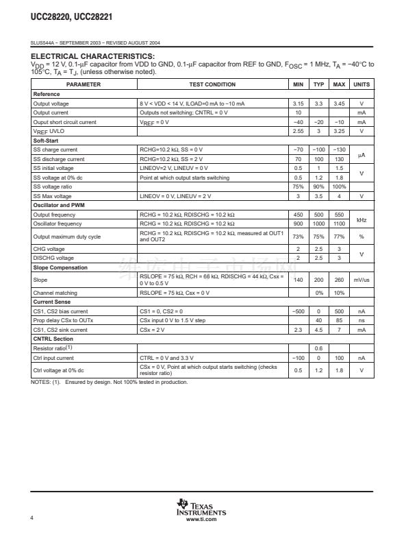
RECOMMENDED OPERATION CONDITIONS
Parameter
High voltage start-up input
Supply voltage
Symbol
VIN
VDD
Condition
36 V to 76 V
8 V to 14.5 V
2
www.ti.com


 1
1
 2
2
 3
3
 4
4
 5
5
 6
6
 7
7
 8
8
 9
9
 10
10
 11
11
 12
12
 13
13
 14
14
 15
15
 16
16
 17
17
 18
18
 19
19
 20
20
 21
21
 22
22
 23
23
 24
24
