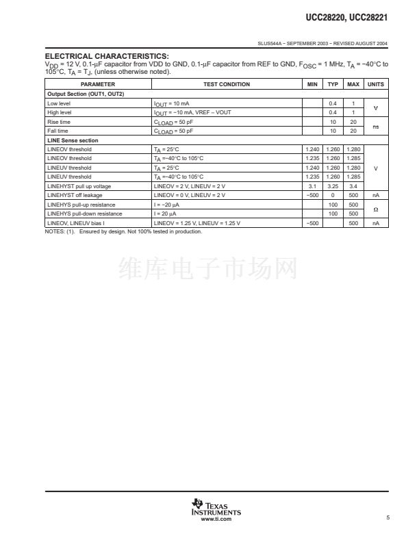
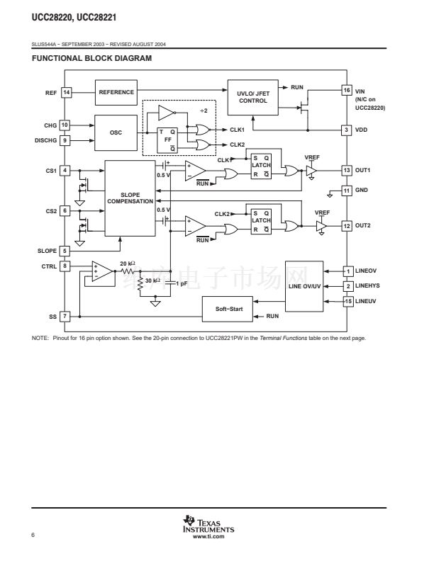
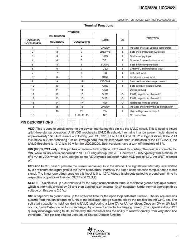
UCC28220, UCC28221
SLUS544A 鈭?SEPTEMBER 2003 鈭?REVISED AUGUST 2004
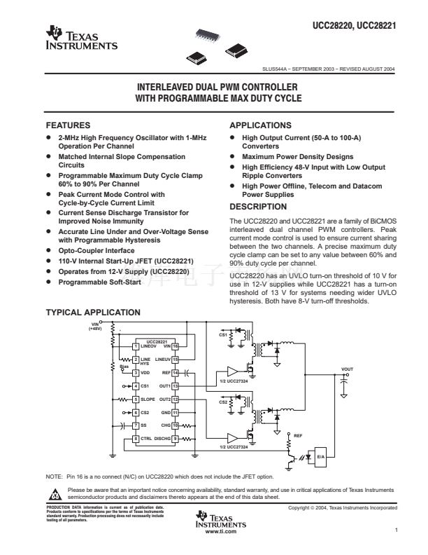
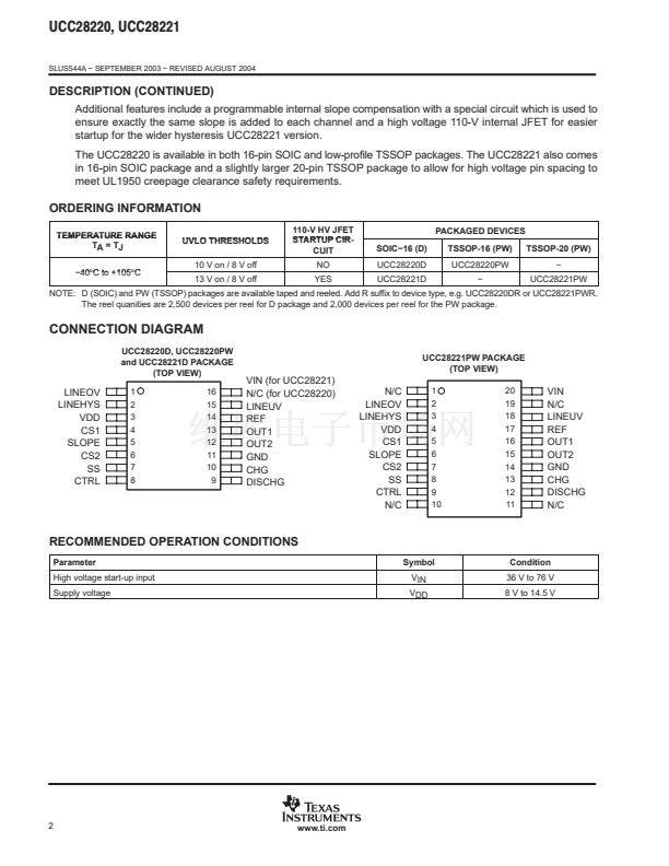
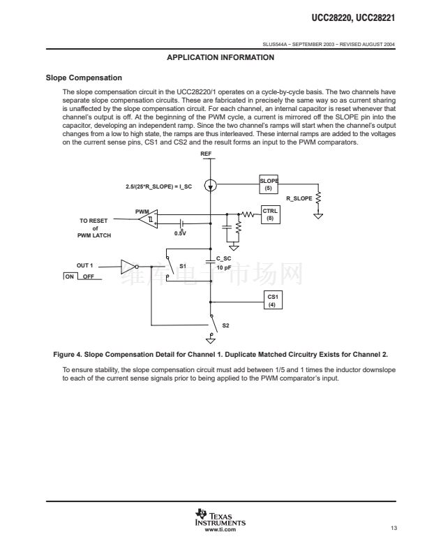
APPLICATION INFORMATION
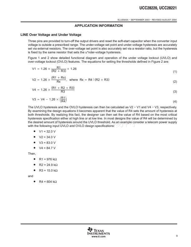
Input
Voltage
R1
UV
15
1.26 V
+
S1
OPEN
HYS
2
R4
S2
CLOSED
R2
LINE_GOOD
1.26 V
+
OV
1
R3
1.26 V
+
Figure 1. Line UVLO and OVLO Functional Diagram
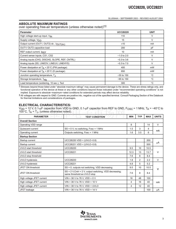
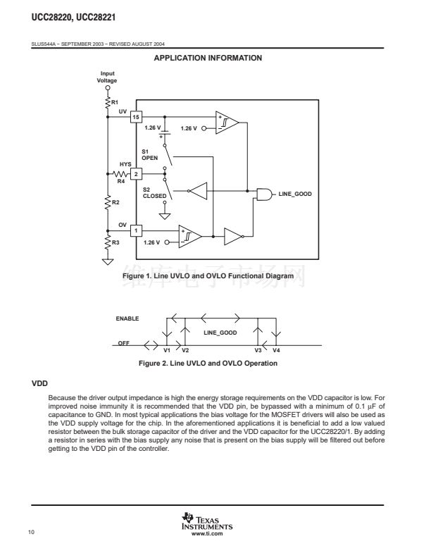
ENABLE
LINE_GOOD
OFF
V1
V2
V3
V4
Figure 2. Line UVLO and OVLO Operation
VDD
Because the driver output impedance is high the energy storage requirements on the VDD capacitor is low. For
improved noise immunity it is recommended that the VDD pin, be bypassed with a minimum of 0.1
碌F
of
capacitance to GND. In most typical applications the bias voltage for the MOSFET drivers will also be used as
the VDD supply voltage for the chip. In the aforementioned applications it is beneficial to add a low valued
resistor between the bulk storage capacitor of the driver and the VDD capacitor for the UCC28220/1. By adding
a resistor in series with the bias supply any noise that is present on the bias supply will be filtered out before
getting to the VDD pin of the controller.
10
www.ti.com


 1
1
 2
2
 3
3
 4
4
 5
5
 6
6
 7
7
 8
8
 9
9
 10
10
 11
11
 12
12
 13
13
 14
14
 15
15
 16
16
 17
17
 18
18
 19
19
 20
20
 21
21
 22
22
 23
23
 24
24
