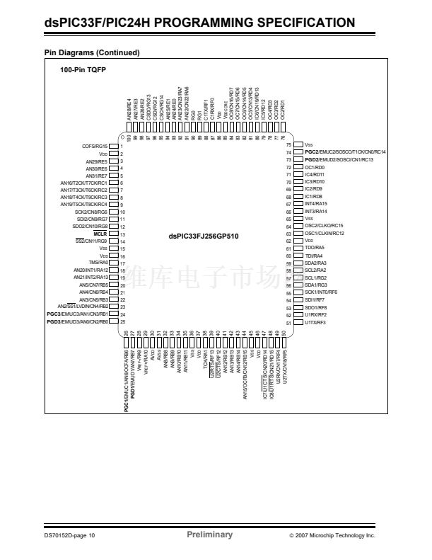
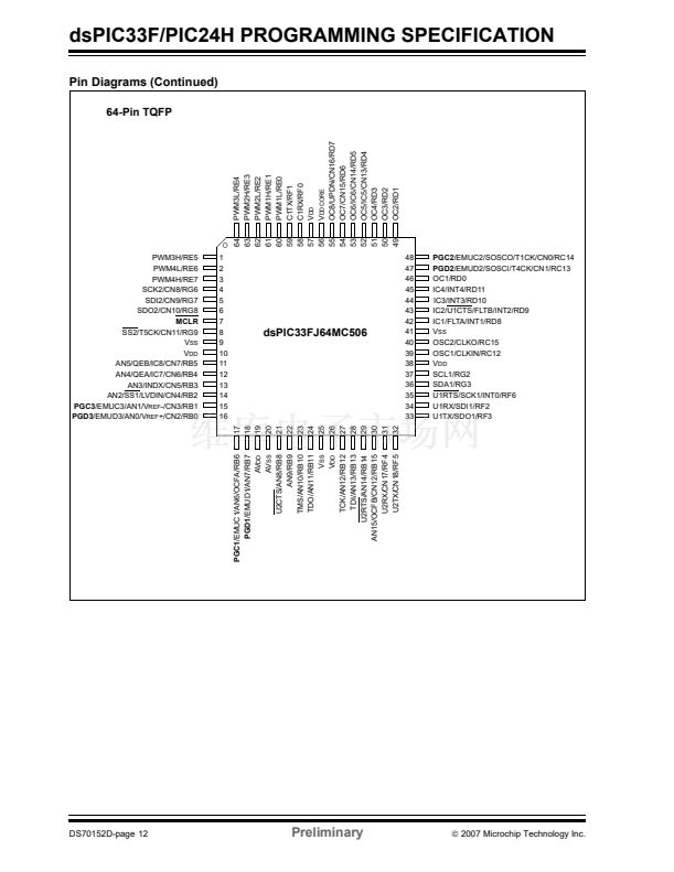
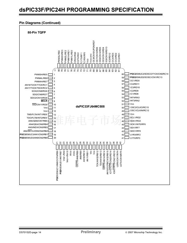
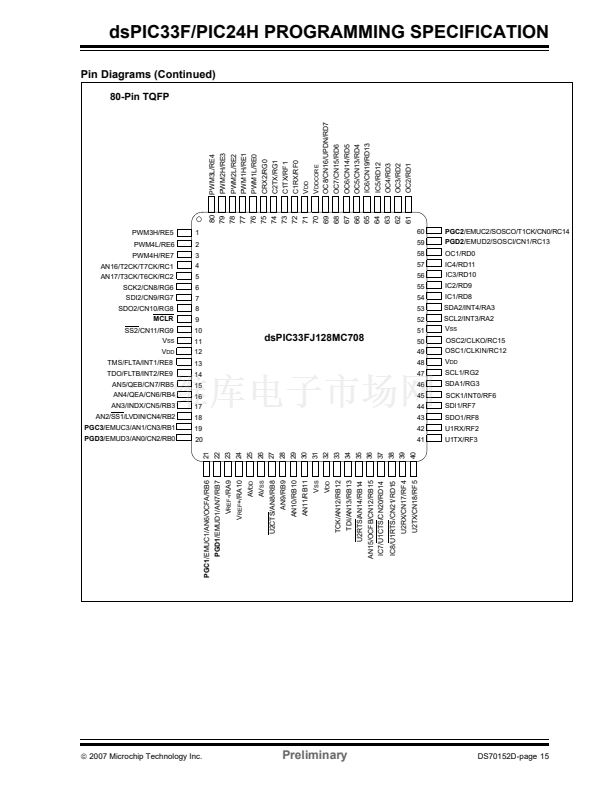
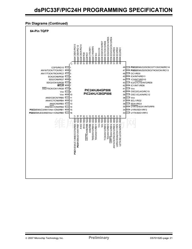
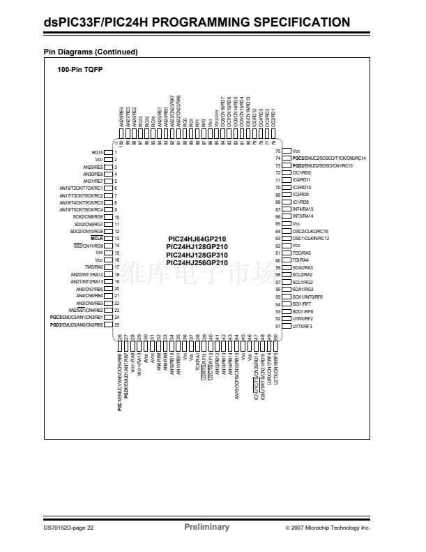
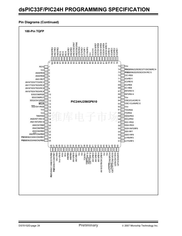
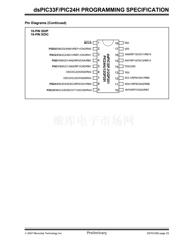
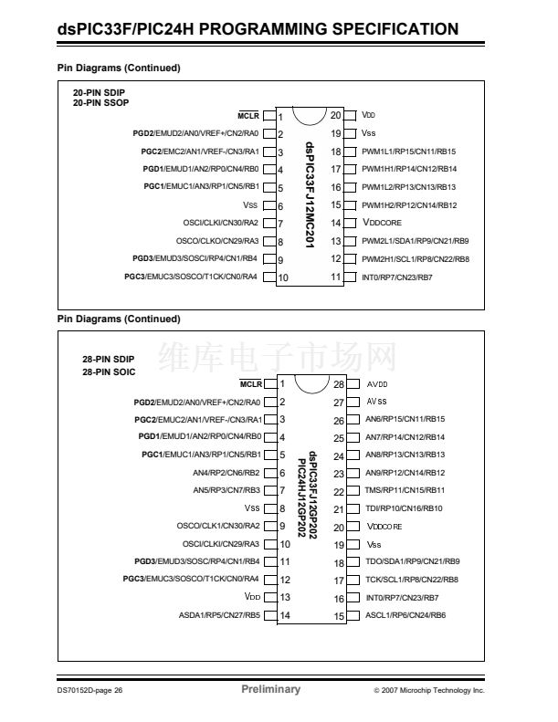
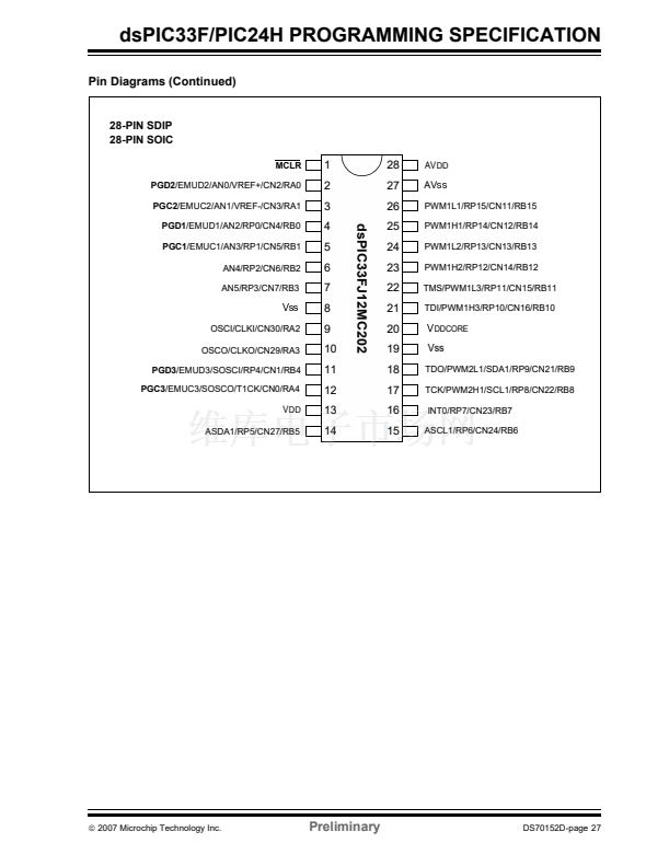
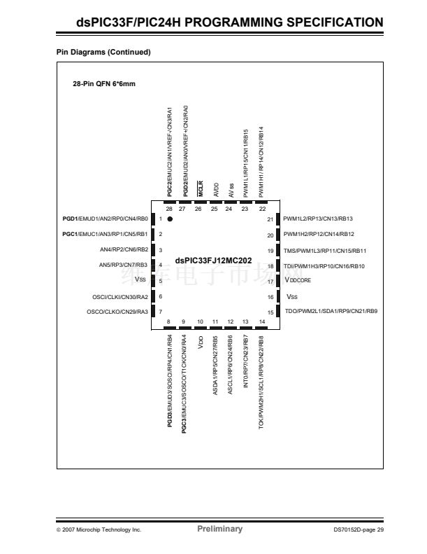
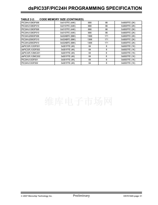
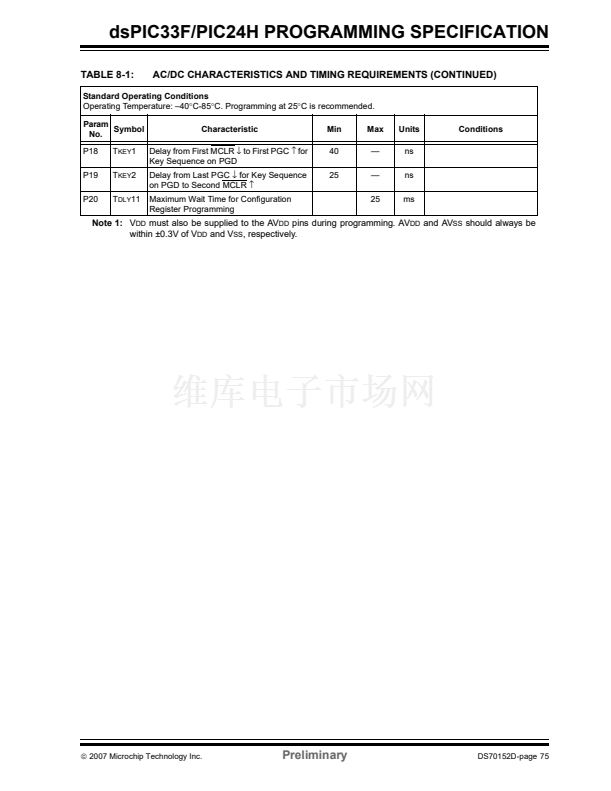
dsPIC33F/PIC24H PROGRAMMING SPECIFICATION
5.7
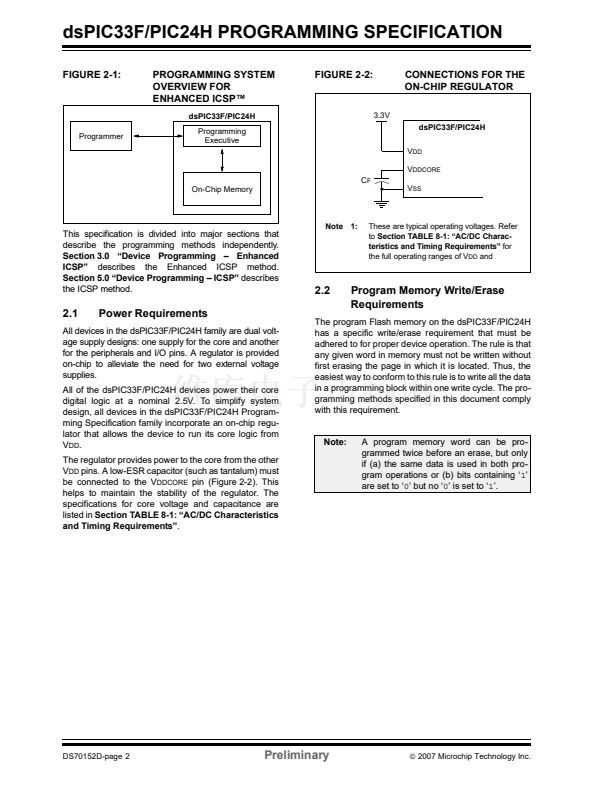
Writing Configuration Memory
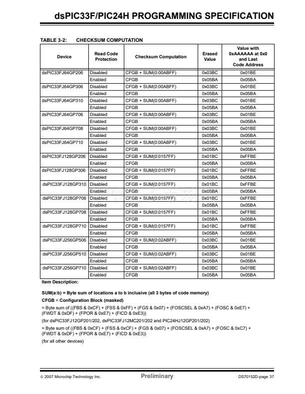
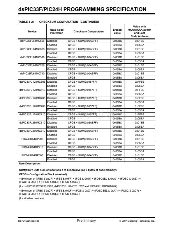
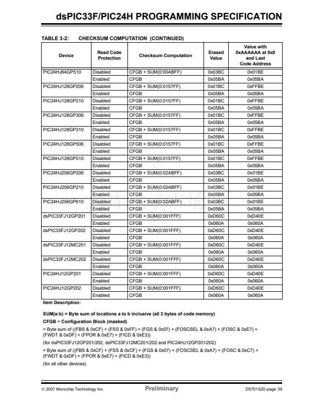
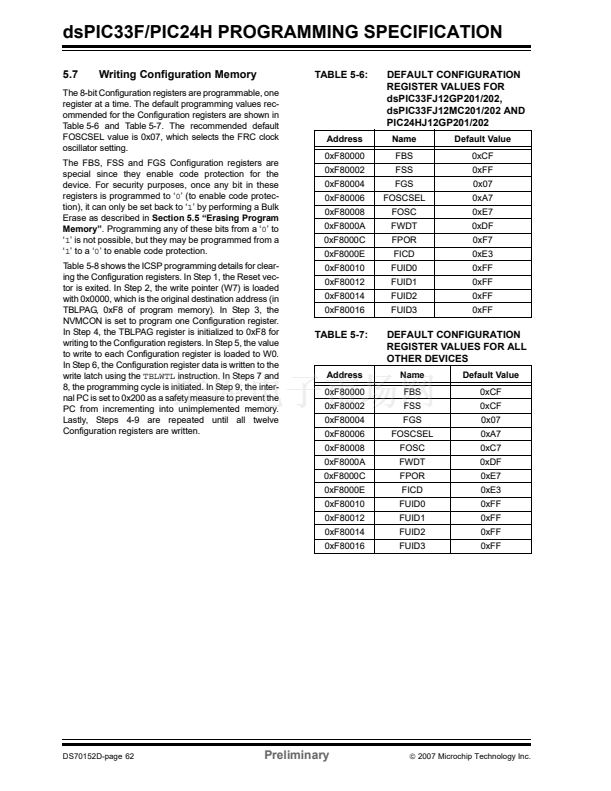
TABLE 5-6:
DEFAULT CONFIGURATION
REGISTER VALUES FOR
dsPIC33FJ12GP201/202,
dsPIC33FJ12MC201/202 AND
PIC24HJ12GP201/202
Name
FBS
FSS
FGS
FOSCSEL
FOSC
FWDT
FPOR
FICD
FUID0
FUID1
FUID2
FUID3
Default Value
0xCF
0xFF
0x07
0xA7
0xE7
0xDF
0xF7
0xE3
0xFF
0xFF
0xFF
0xFF
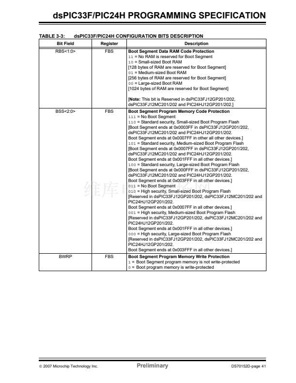
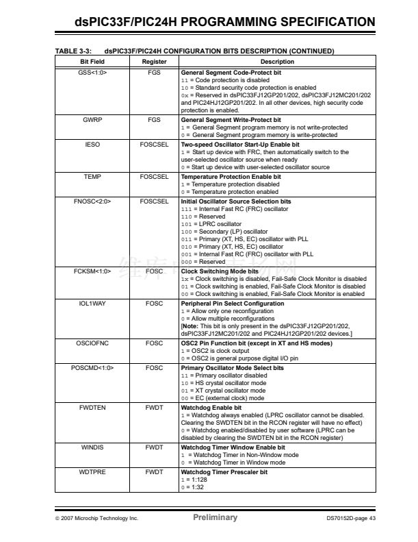
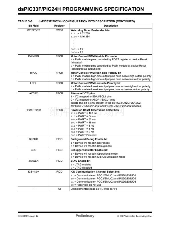
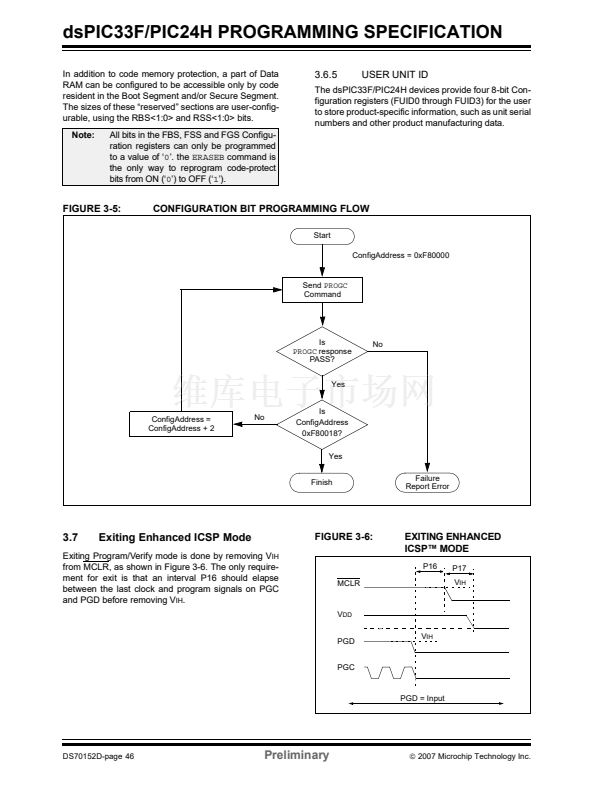
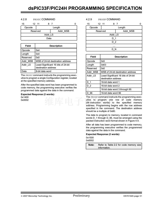
The 8-bit Configuration registers are programmable, one
register at a time. The default programming values rec-
ommended for the Configuration registers are shown in
Table 5-6 and Table 5-7. The recommended default
FOSCSEL value is 0x07, which selects the FRC clock
oscillator setting.
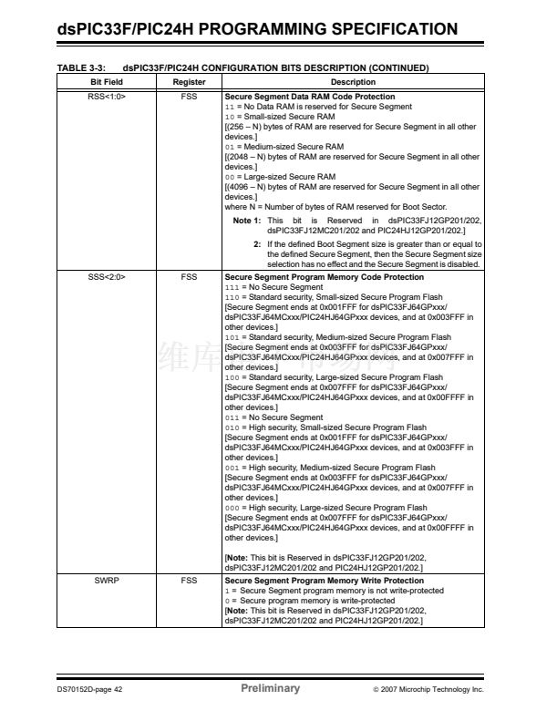
The FBS, FSS and FGS Configuration registers are
special since they enable code protection for the
device. For security purposes, once any bit in these
registers is programmed to 鈥?鈥?(to enable code protec-
tion), it can only be set back to 鈥?鈥?by performing a Bulk
Erase as described in
Section 5.5 鈥淓rasing Program
Memory鈥?
Programming any of these bits from a 鈥?鈥?to
鈥?鈥?is not possible, but they may be programmed from a
鈥?鈥?to a 鈥?鈥?to enable code protection.
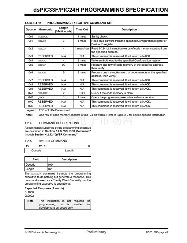
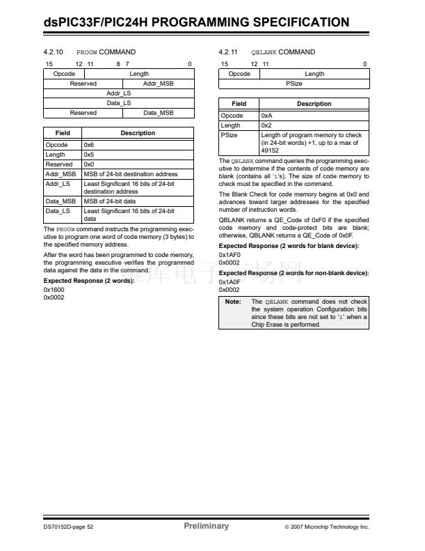
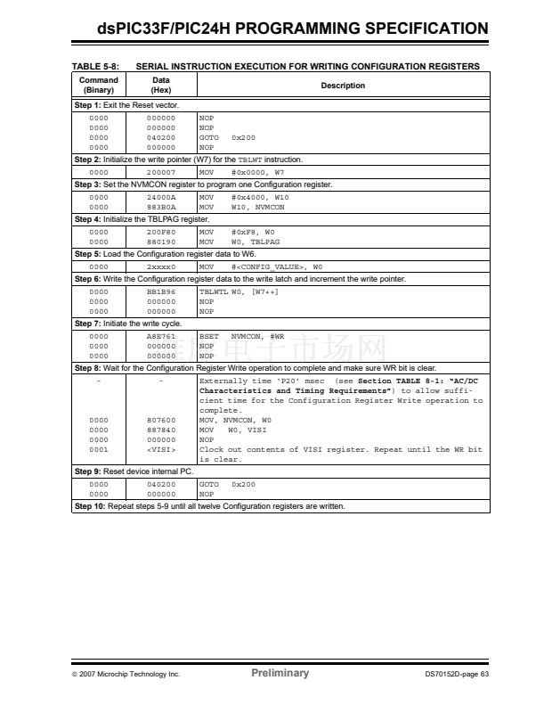
Table 5-8 shows the ICSP programming details for clear-
ing the Configuration registers. In Step 1, the Reset vec-
tor is exited. In Step 2, the write pointer (W7) is loaded
with 0x0000, which is the original destination address (in
TBLPAG, 0xF8 of program memory). In Step 3, the
NVMCON is set to program one Configuration register.
In Step 4, the TBLPAG register is initialized to 0xF8 for
writing to the Configuration registers. In Step 5, the value
to write to each Configuration register is loaded to W0.
In Step 6, the Configuration register data is written to the
write latch using the
TBLWTL
instruction. In Steps 7 and
8, the programming cycle is initiated. In Step 9, the inter-
nal PC is set to 0x200 as a safety measure to prevent the
PC from incrementing into unimplemented memory.
Lastly, Steps 4-9 are repeated until all twelve
Configuration registers are written.
Address
0xF80000
0xF80002
0xF80004
0xF80006
0xF80008
0xF8000A
0xF8000C
0xF8000E
0xF80010
0xF80012
0xF80014
0xF80016
TABLE 5-7:
DEFAULT CONFIGURATION
REGISTER VALUES FOR ALL
OTHER DEVICES
Name
FBS
FSS
FGS
FOSCSEL
FOSC
FWDT
FPOR
FICD
FUID0
FUID1
FUID2
FUID3
Default Value
0xCF
0xCF
0x07
0xA7
0xC7
0xDF
0xE7
0xE3
0xFF
0xFF
0xFF
0xFF
Address
0xF80000
0xF80002
0xF80004
0xF80006
0xF80008
0xF8000A
0xF8000C
0xF8000E
0xF80010
0xF80012
0xF80014
0xF80016
DS70152D-page 62
Preliminary
漏
2007 Microchip Technology Inc.


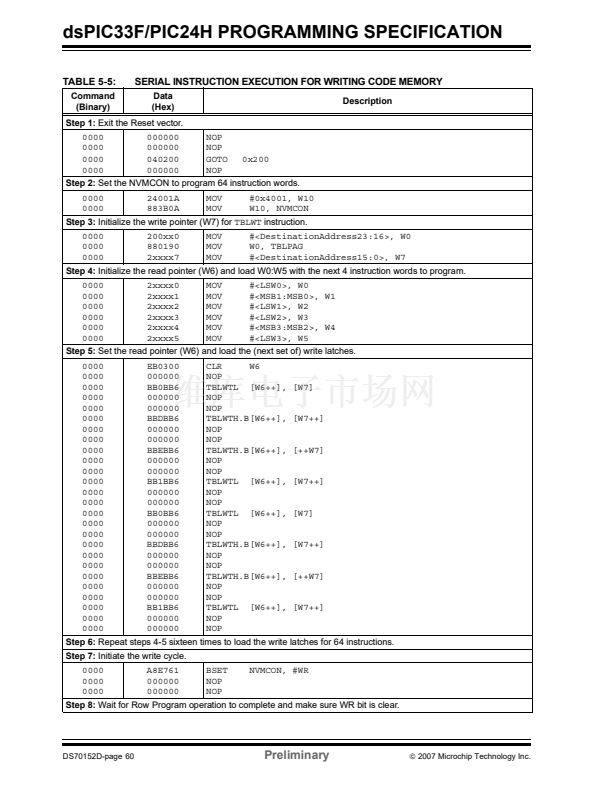
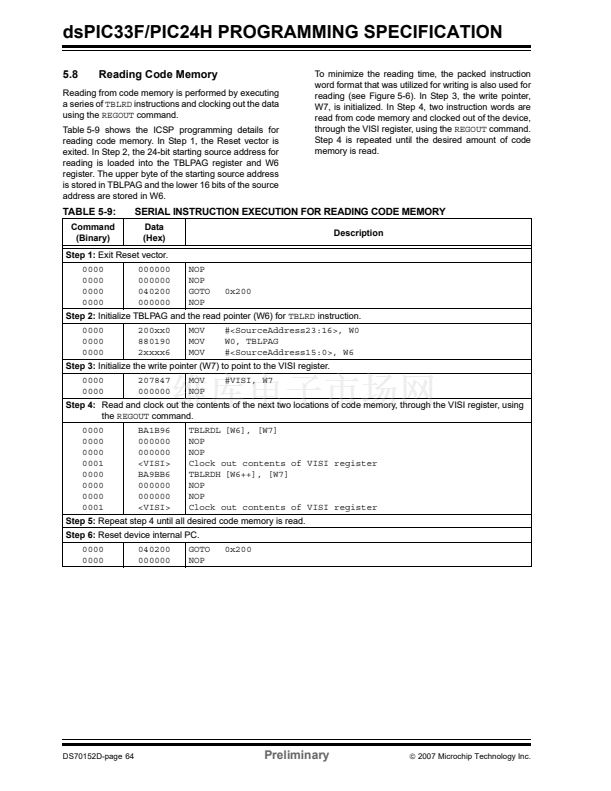
 1
1
 2
2
 3
3
 4
4
 5
5
 6
6
 7
7
 8
8
 9
9
 10
10
 11
11
 12
12
 13
13
 14
14
 15
15
 16
16
 17
17
 18
18
 19
19
 20
20
 21
21
 22
22
 23
23
 24
24
 25
25
 26
26
 27
27
 28
28
 29
29
 30
30
 31
31
 32
32
 33
33
 34
34
 35
35
 36
36
 37
37
 38
38
 39
39
 40
40
 41
41
 42
42
 43
43
 44
44
 45
45
 46
46
 47
47
 48
48
 49
49
 50
50
 51
51
 52
52
 53
53
 54
54
 55
55
 56
56
 57
57
 58
58
 59
59
 60
60
 61
61
 62
62
 63
63
 64
64
 65
65
 66
66
 67
67
 68
68
 69
69
 70
70
 71
71
 72
72
 73
73
 74
74
 75
75
 76
76
 77
77
 78
78
 79
79
 80
80
