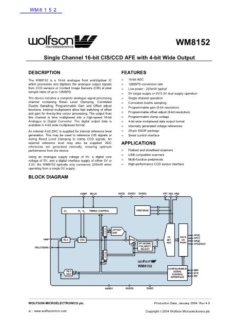
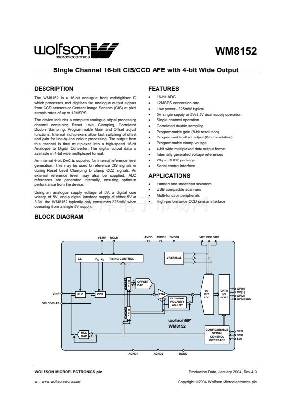
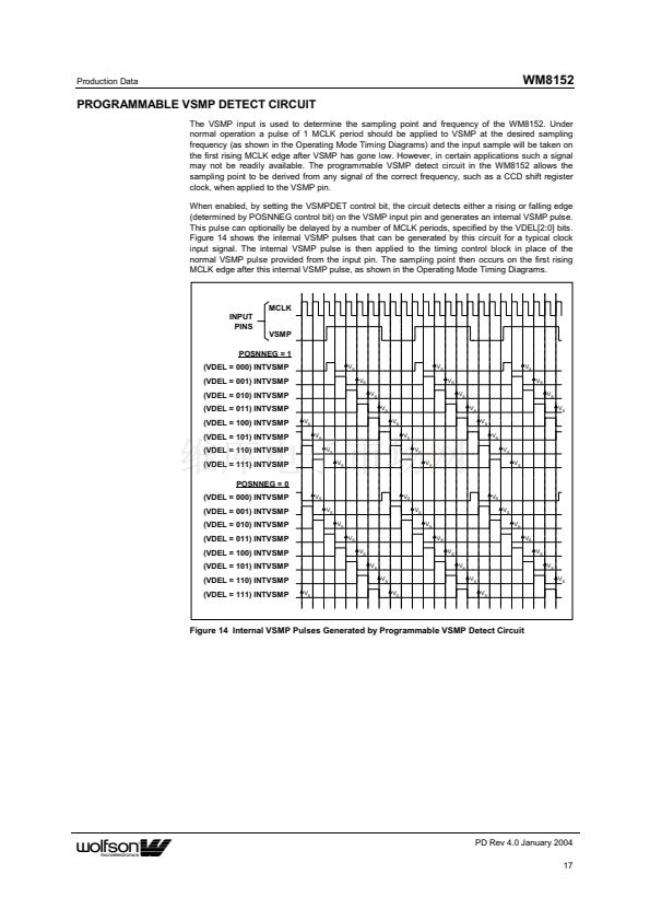
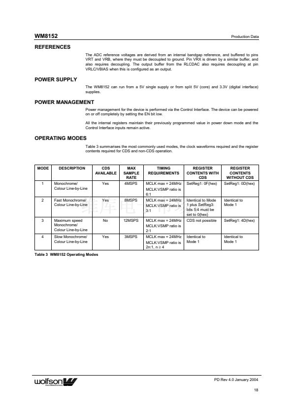
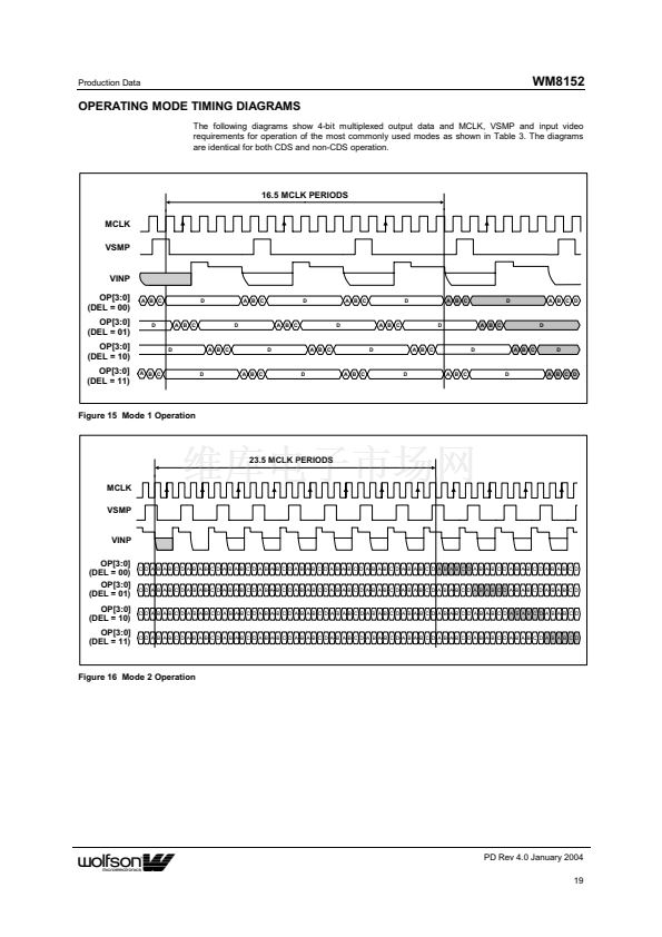
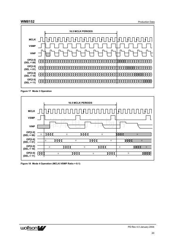
WM8152
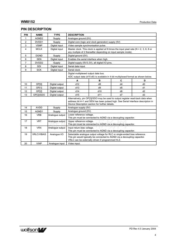
PIN DESCRIPTION
PIN
1
2
3
4
5
6
7
8
9
NAME
AGND2
DVDD1
VSMP
MCLK
DGND
SEN
DVDD2
SDI
SCK
TYPE
Supply
Supply
Digital input
Digital input
Supply
Digital input
Supply
Digital input
Digital input
DESCRIPTION
Analogue ground (0V).
Digital core (logic and clock generator) supply (5V)
Video sample synchronisation pulse.
Production Data
Master clock. This clock is applied at N times the input pixel rate (N = 2, 3, 6, 8 or
any multiple of 2 thereafter depending on input sample mode).
Digital ground (0V).
Enables the serial interface when high.
Digital supply (5V/3.3V), all digital I/O pins.
Serial data input.
Serial clock.
Digital multiplexed output data bus.
ADC output data (d15:d0) is available in 4-bit multiplexed format as shown below.
A
B
d8
d9
d10
d11
C
d4
d5
d6
d7
D
d0
d1
d2
d3
10
11
12
13
OP[0]
OP[1]
OP[2]
OP[3]/SDO
Digital output
Digital output
Digital output
Digital output
d12
d13
d14
d15
Alternatively, pin OP[3]/SDO may be used to output register read-back data when
address bit 4=1 and SEN has been pulsed high. See Serial Interface description in
Device Description section for further details.
14
15
16
17
18
19
AVDD
AGND1
VRB
VRT
VRX
VRLC/VBIAS
Supply
Supply
Analogue output
Analogue output
Analogue output
Analogue I/O
Analogue supply (5V)
Analogue ground (0V).
Lower reference voltage.
This pin must be connected to AGND via a decoupling capacitor.
Upper reference voltage.
This pin must be connected to AGND via a decoupling capacitor.
Input return bias voltage.
This pin must be connected to AGND via a decoupling capacitor.
Selectable analogue output voltage for RLC or single-ended bias reference.
This pin would typically be connected to AGND via a decoupling capacitor.
VRLC can be externally driven if programmed Hi-Z.
Video input.
20
VINP
Analogue input
w
PD Rev 4.0 January 2004
4


 1
1
 2
2
 3
3
 4
4
 5
5
 6
6
 7
7
 8
8
 9
9
 10
10
 11
11
 12
12
 13
13
 14
14
 15
15
 16
16
 17
17
 18
18
 19
19
 20
20
 21
21
 22
22
 23
23
 24
24
 25
25
 26
26
