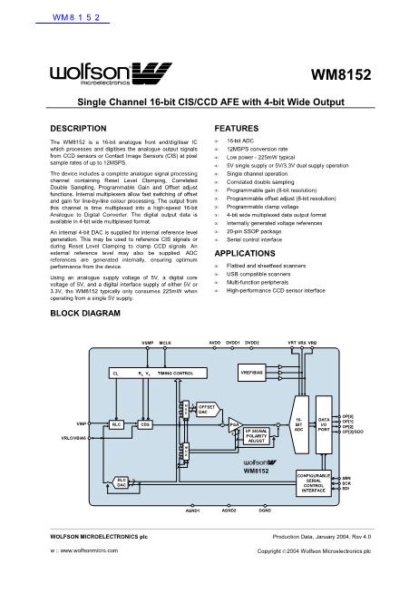
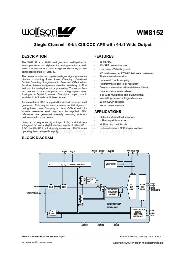
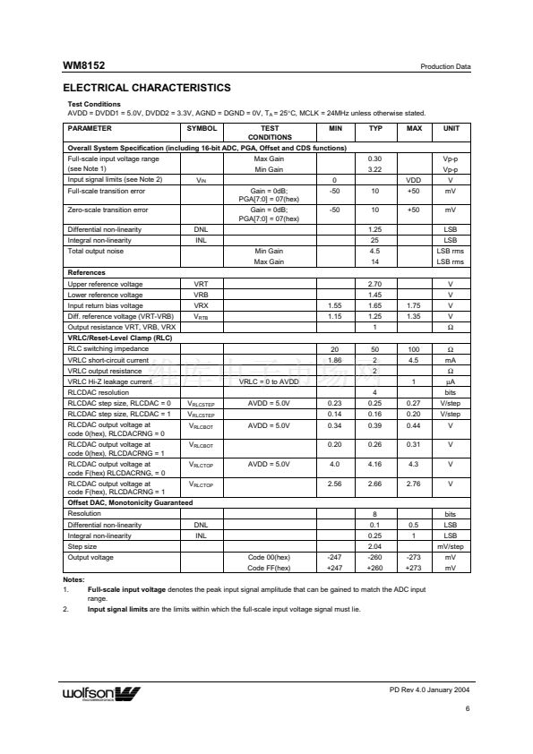
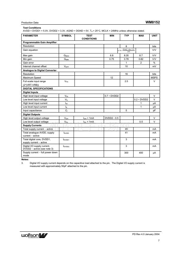
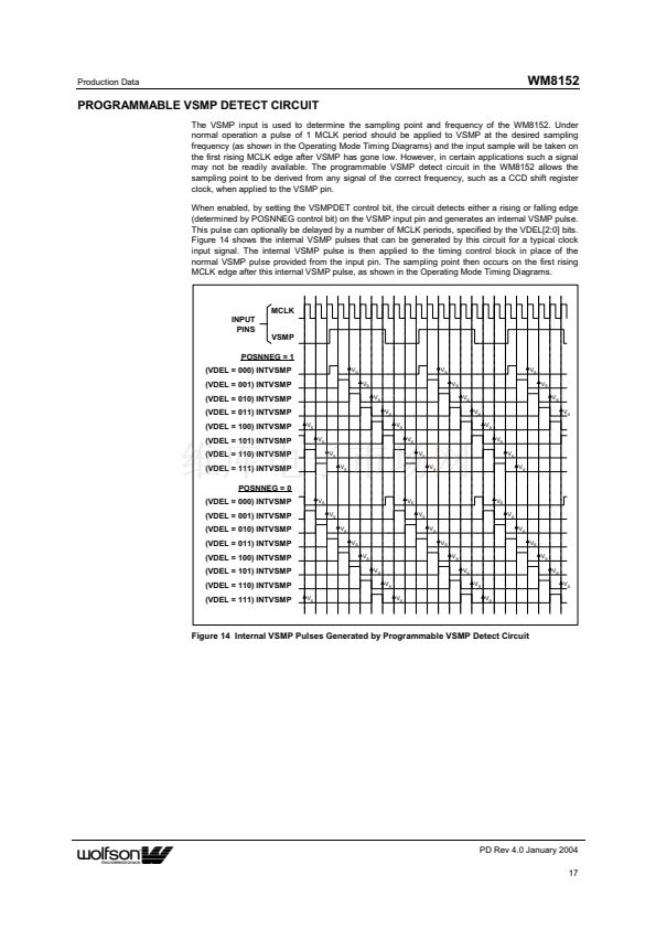
WM8152
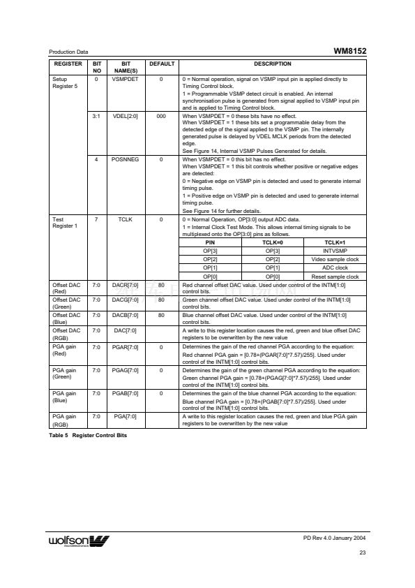
REGISTER MAP DESCRIPTION
Production Data
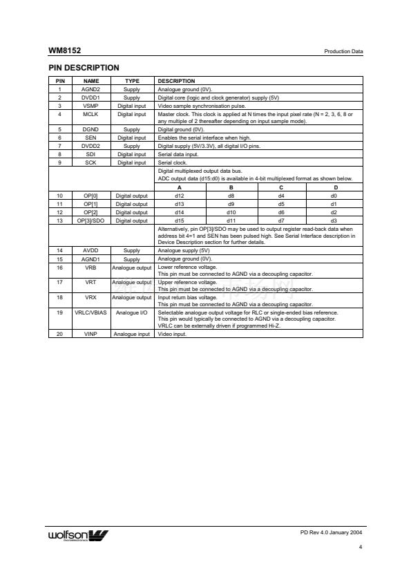
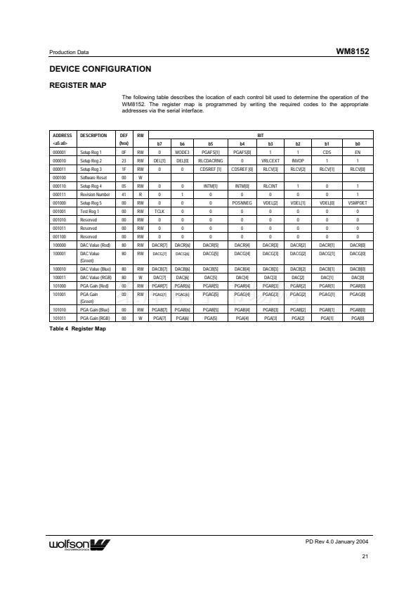
The following table describes the function of each of the control bits shown in Table 4.
REGISTER
Setup
Register 1
BIT
NO
0
1
5:4
BIT
NAME(S)
EN
CDS
PGAFS[1:0]
DEFAULT
1
1
00
DESCRIPTION
0 = complete power down, 1 = fully active.
Select correlated double sampling mode: 0 = single ended mode,
1 = CDS mode.
Offsets PGA output to optimise the ADC range for different polarity sensor
output signals. Zero differential PGA input signal gives:
00 = Zero output
(use for bipolar video)
01 = Zero output
6
Setup
Register 2
2
MODE3
INVOP
0
0
10 = Full-scale positive output
(use for negative going video)
11 = Full-scale negative output
(use for positive going video)
Required when operating in MODE3: 0 = other modes, 1 = MODE3.
Digitally inverts the polarity of output data.
0 = negative going video gives negative going output,
1 = negative-going video gives positive going output data.
When set powers down the RLCDAC, changing its output to Hi-Z, allowing
VRLC/VBIAS to be externally driven.
Sets the output range of the RLCDAC.
0 = RLCDAC ranges from 0 to VDD (approximately),
1 = RLCDAC ranges from 0 to VRT (approximately).
Sets the output latency in ADC clock periods.
1 ADC clock period = 2 MCLK periods except in Mode 2 where 1 ADC
clock period = 3 MCLK periods.
00 = Minimum latency
01 = Delay by one ADC clock
period
10 = Delay by two ADC clock periods
11 = Delay by three ADC clock
periods
3
5
VRLCEXT
RLCDACRNG
0
1
7:6
DEL[1:0]
00
Setup
Register 3
3:0
RLCV[3:0]
1111
Controls RLCDAC driving VRLC pin to define single ended signal
reference voltage or Reset Level Clamp voltage. See Electrical
Characteristics section for ranges.
CDS mode reset timing adjust.
00 = Advance 1 MCLK period
01 = Normal
10 = Retard 1 MCLK period
11 = Retard 2 MCLK periods
5:4
CDSREF[1:0]
01
Software
Reset
Setup
Register 4
3
5:4
RLCINT
INTM[1:0]
0
00
Any write to Software Reset causes all cells to be reset.
It is recommended that a software reset be performed after a power-up
before any other register writes.
This bit is used to determine whether Reset Level Clamping is enabled.
0 = RLC disabled, 1 = RLC enabled.
Colour selection bits used in internal modes.
00 = Red, 01 = Green, 10 = Blue and 11 = Reserved.
See Table 1 for details.
w
PD Rev 4.0 January 2004
22


 1
1
 2
2
 3
3
 4
4
 5
5
 6
6
 7
7
 8
8
 9
9
 10
10
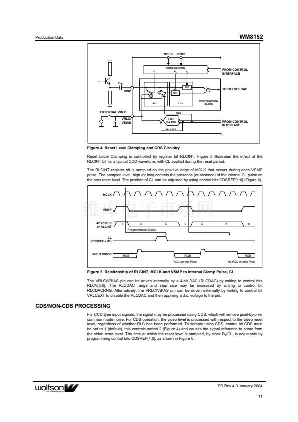 11
11
 12
12
 13
13
 14
14
 15
15
 16
16
 17
17
 18
18
 19
19
 20
20
 21
21
 22
22
 23
23
 24
24
 25
25
 26
26
