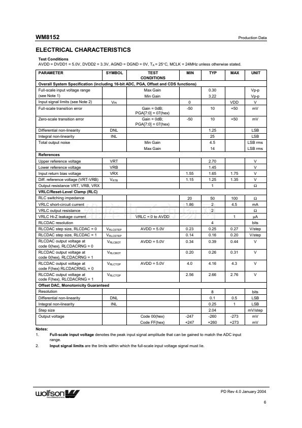
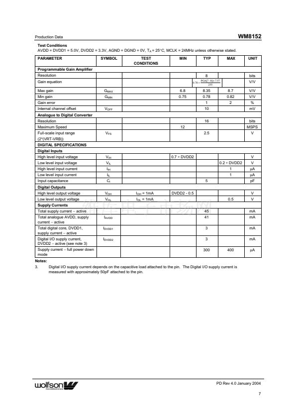
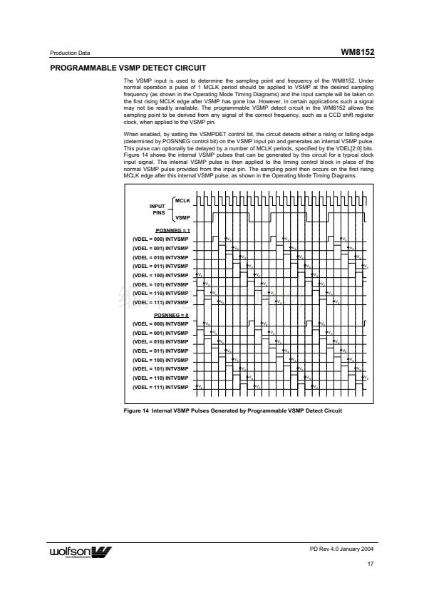
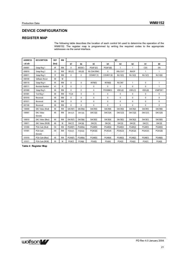
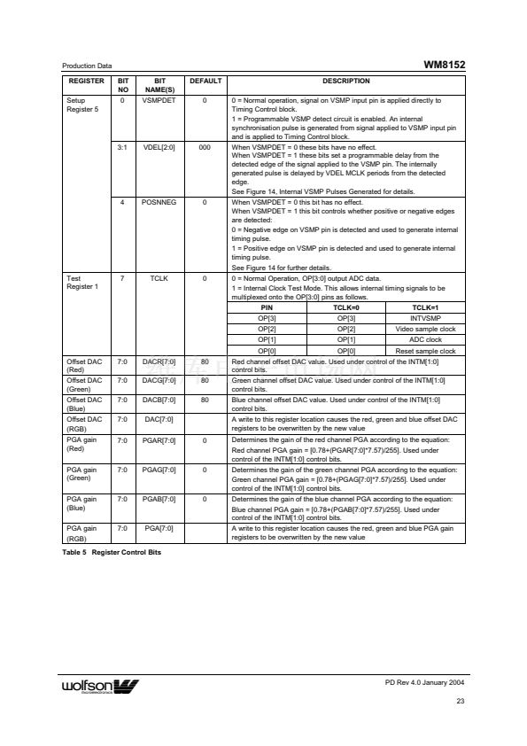
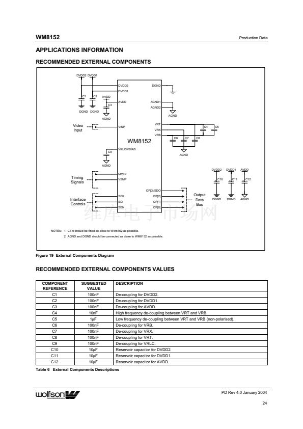
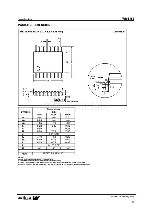
Production Data
WM8152
ADC INPUT BLACK LEVEL ADJUST
The output from the PGA should be offset to match the full-scale range of the ADC (V
FS
= 2.5V). For
negative-going input video signals, a black level (zero differential) output from the PGA should be
offset to the top of the ADC range by setting register bits PGAFS[1:0]=10. For positive going input
signal the black level should be offset to the bottom of the ADC range by setting PGAFS[1:0]=11.
Bipolar input video is accommodated by setting PGAFS[1:0]=00 or PGAFS[1:0]=01 (zero differential
input voltage gives mid-range ADC output).
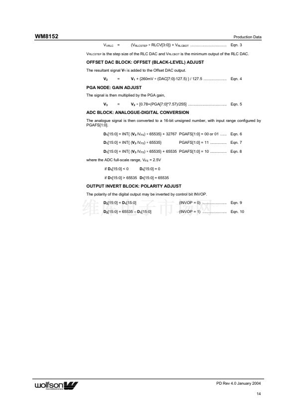
OVERALL SIGNAL FLOW SUMMARY
Figure 9 represents the processing of the video signal through the WM8152.
OUTPUT
INVERT
BLOCK
INPUT
SAMPLING OFFSET DAC PGA
BLOCK
BLOCK
BLOCK
ADC BLOCK
V
1
V
IN
CDS = 1
V
RESET
CDS = 0
V
VRLC
VRLCEXT=1
VRLCEXT=0
V
2
++
+
-
X
V
3
analog
x (65535/V
FS
)
+0
if PGAFS[1:0]=11
+65535 if PGAFS[1:0]=10
+32767 if PGAFS[1:0]=0x
D
1
digital
D
2
OP[3:0]
D2 = D1 if INVOP = 0
D2 =65535-D1 if INVOP = 1
PGA gain
A = 0.78+(PGA[7:0]*7.57)/255
Offset
DAC
260mV*(DAC[7:0]-127.5)/127.5
V
IN
is VINP voltage sampled on video sample
V
RESET
is VINP sampled during reset clamp
V
VRLC
is voltage applied to VRLC pin
CDS, VRLCEXT,RLCV[3:0], DAC[7:0],
PGA[7:0], PGAFS[1:0] and INVOP are set
by programming internal control registers.
CDS=1 for CDS, 0 for non-CDS
RLC
DAC
V
RLCSTEP
*RLCV[3:0] + V
RLCBOT
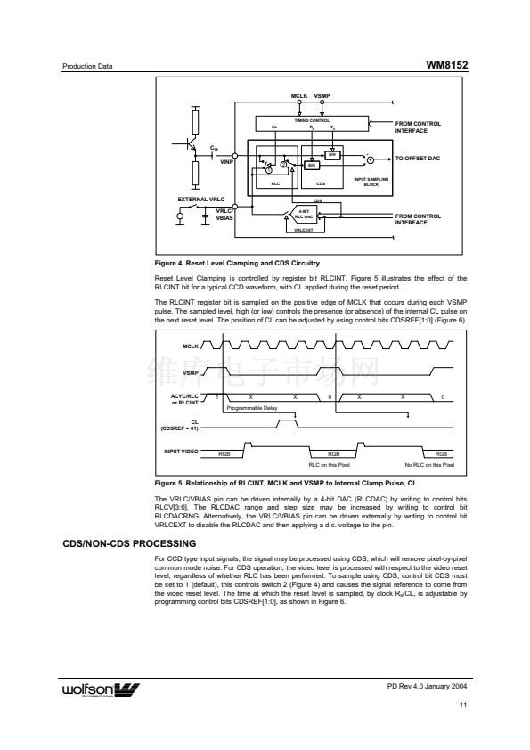
Figure 9 Overall Signal Flow
The
INPUT SAMPLING BLOCK
produces an effective input voltage
V
1
. For CDS, this is the
difference between the input video level V
IN
and the input reset level V
RESET
. For non-CDS this is the
difference between the input video level V
IN
and the voltage on the VRLC/VBIAS pin, V
VRLC
,
optionally set via the RLC DAC.
The
OFFSET DAC BLOCK
then adds the amount of fine offset adjustment required to move the
black level of the input signal towards 0V, producing
V
2
.
The
PGA BLOCK
then amplifies the white level of the input signal to maximise the ADC range,
outputting voltage
V
3
.
The
ADC BLOCK
then converts the analogue signal,
V
3
, to a 16-bit unsigned digital output,
D
1
.
The digital output is then inverted, if required, through the
OUTPUT INVERT BLOCK
to produce
D
2.
CALCULATING OUTPUT FOR ANY GIVEN INPUT
The following equations describe the processing of the video and reset level signals through
the WM8152.
INPUT SAMPLING BLOCK: INPUT SAMPLING AND REFERENCING
If CDS = 1, (i.e. CDS operation) the previously sampled reset level, V
RESET
, is subtracted from the
input video.
V
1
=
V
IN
- V
RESET
...................................................................
Eqn. 1
If CDS = 0, (non-CDS operation) the simultaneously sampled voltage on pin VRLC is subtracted
instead.
V
1
=
V
IN
- V
VRLC
....................................................................
Eqn. 2
If VRLCEXT = 1, V
VRLC
is an externally applied voltage on pin VRLC/VBIAS.
If VRLCEXT = 0, V
VRLC
is the output from the internal RLC DAC.
w
PD Rev 4.0 January 2004
13


 1
1
 2
2
 3
3
 4
4
 5
5
 6
6
 7
7
 8
8
 9
9
 10
10
 11
11
 12
12
 13
13
 14
14
 15
15
 16
16
 17
17
 18
18
 19
19
 20
20
 21
21
 22
22
 23
23
 24
24
 25
25
 26
26
