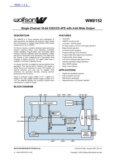
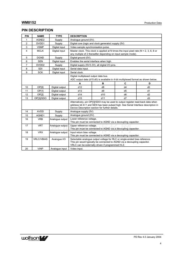
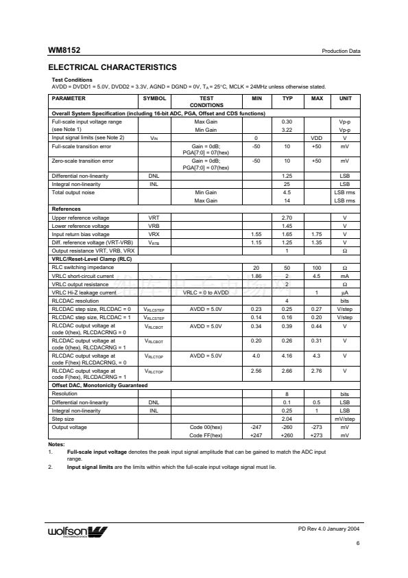
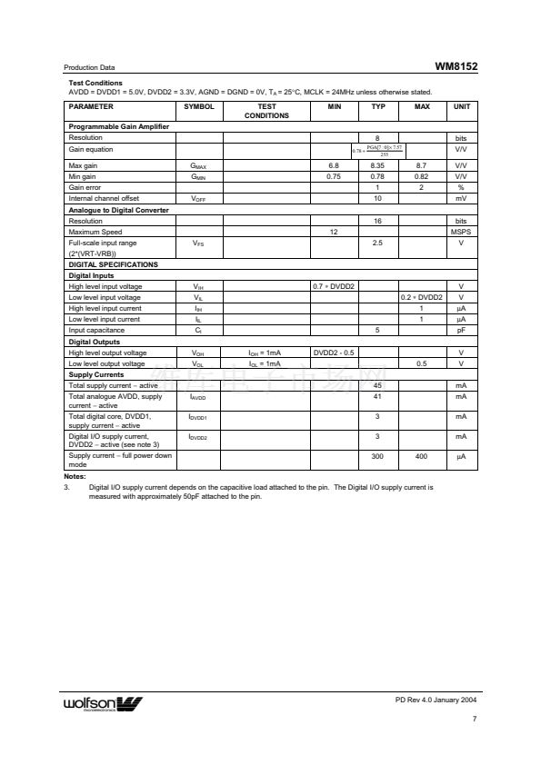
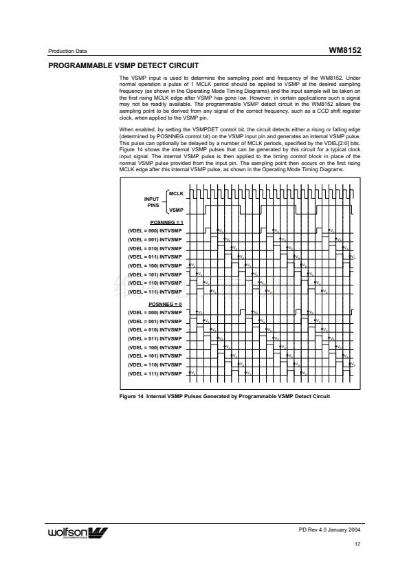
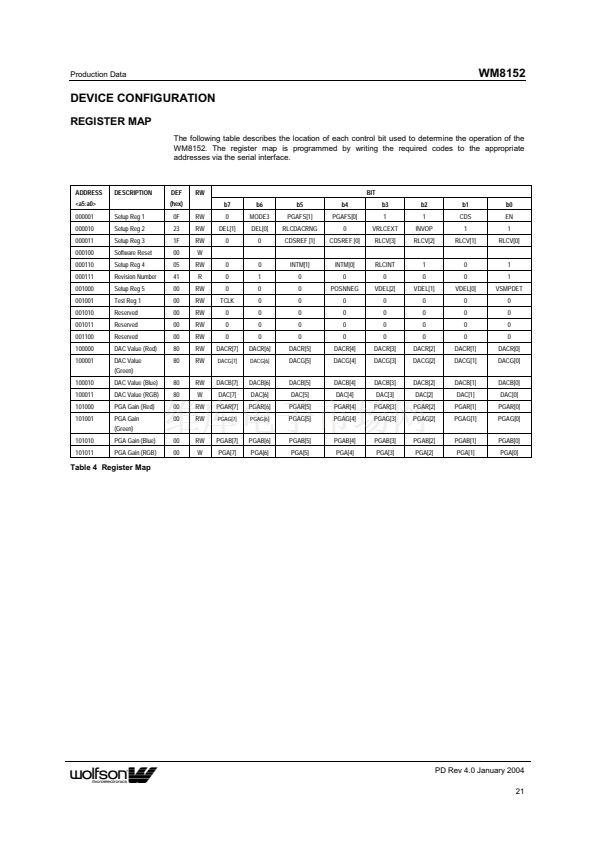
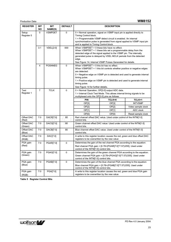
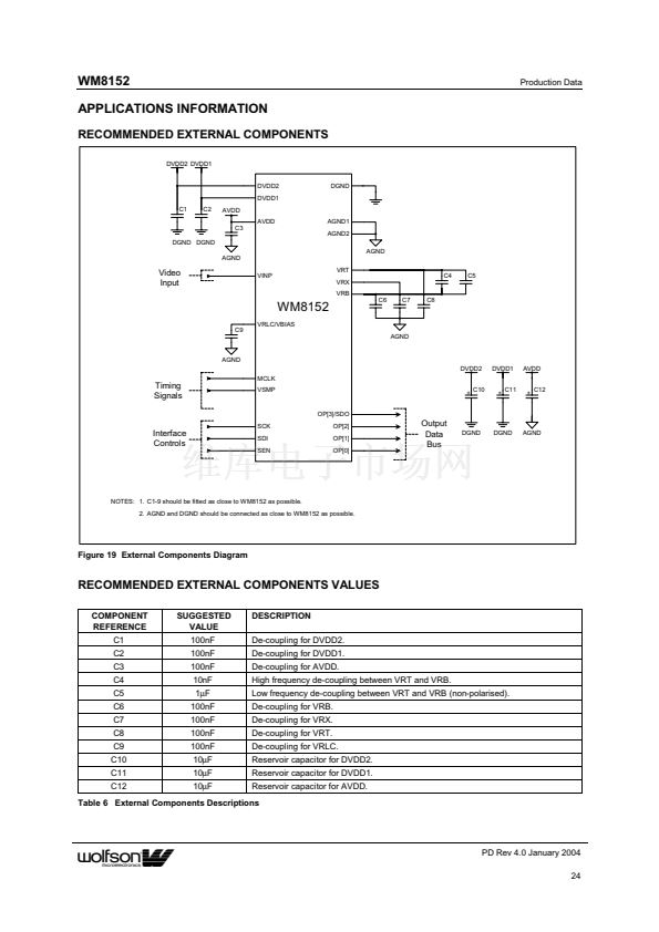
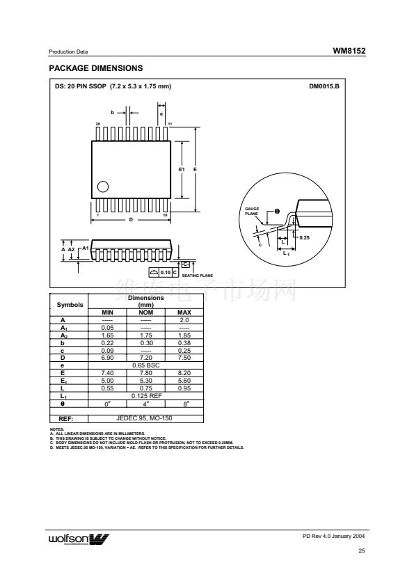
WM8152
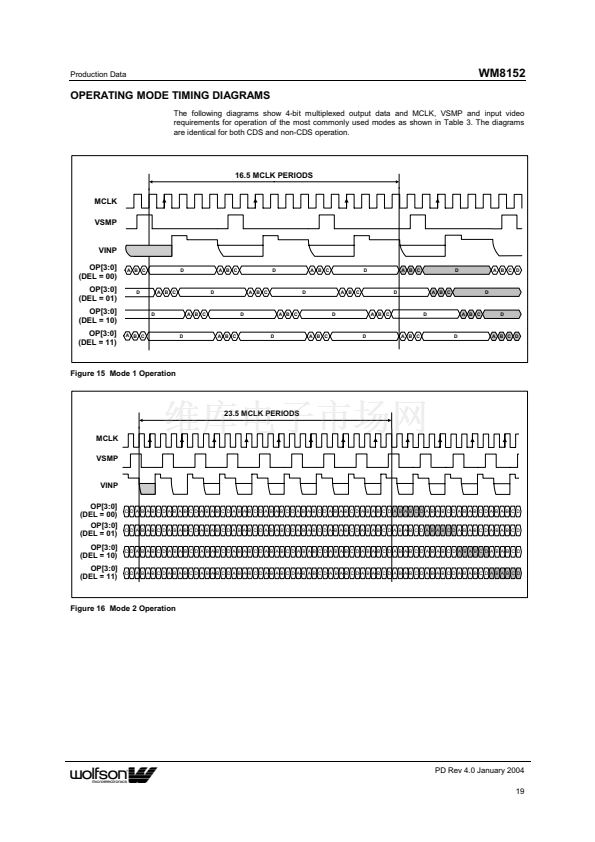
Production Data
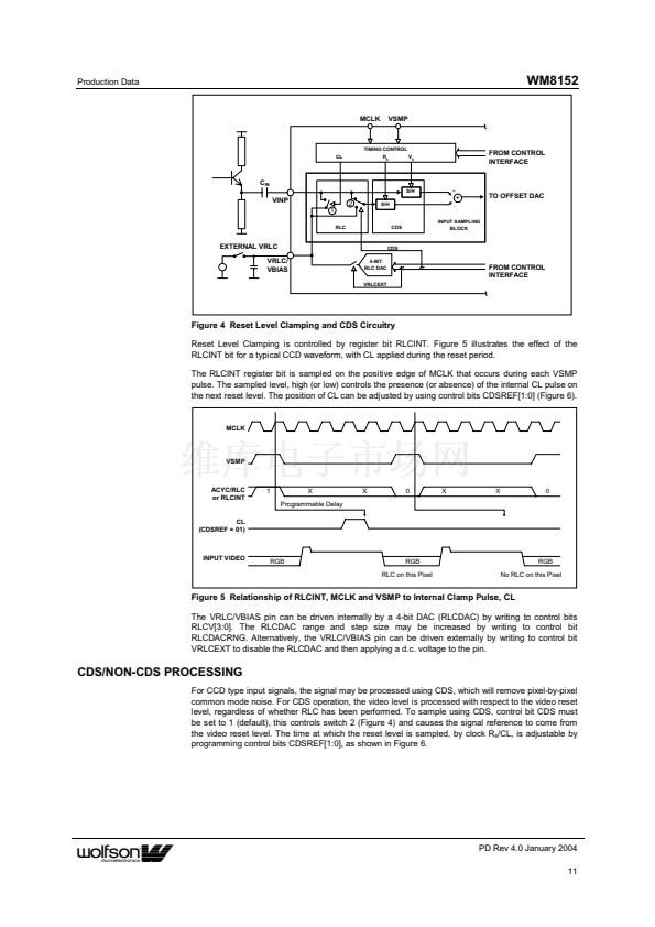
MCLK
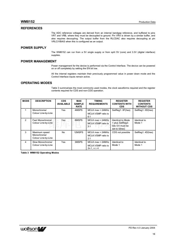
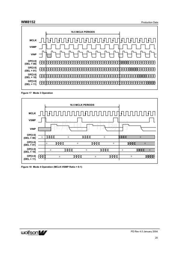
VSMP
VS
R
S
/CL (CDSREF = 00)
R
S
/CL (CDSREF = 01)
R
S
/CL (CDSREF = 10)
R
S
/CL (CDSREF = 11)
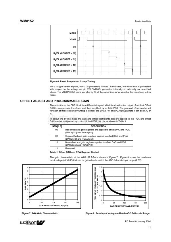
Figure 6 Reset Sample and Clamp Timing
For CIS type sensor signals, non-CDS processing is used. In this case, the video level is processed
with respect to the voltage on pin VRLC/VBIAS, generated internally or externally as described
above. The VRLC/VBIAS pin is sampled by R
s
at the same time as V
s
samples the video level in this
mode.
OFFSET ADJUST AND PROGRAMMABLE GAIN
The output from the CDS block is a differential signal, which is added to the output of an 8-bit Offset
DAC to compensate for offsets and then amplified by an 8-bit PGA. The gain and offset can be set
for each of three colours by writing to control bits DACx[7:0] and PGAx[7:0] (where x can be R, G or
B).
In colour line-by-line mode the gain and offset coefficients that are applied to the PGA and offset
DAC can be multiplexed by control of the INTM[1:0] bits as shown in Table 1.
INTM[1:0]
00
01
10
11
DESCRIPTION
Red offset and gain registers are applied to offset DAC and PGA
(DACR[7:0] and PGAR[7:0])
Green offset and gain registers applied to offset DAC and PGA
(DACG[7:0] and PGAG[7:0])
Blue offset and gain registers applied to offset DAC and PGA
(DACB[7:0] and PGAB[7:0])
Reserved.
Table 1 Offset DAC and PGA Register Control
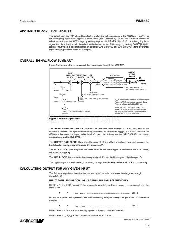
The gain characteristic of the WM8152 PGA is shown in Figure 7. Figure 8 shows the maximum
input voltage (at VINP) that can be gained up to match the ADC full-scale input range (2.5V).
9
8
7
PGA GAIN V/V
6
5
4
3
2
1
0
0
64
128
192
256
GAIN REGISTER VALUE, PGA[7:0]
3.5
3
2.5
2
1.5
1
0.5
0
0
64
128
192
256
GAIN REGISTER VALUE, PGA[7:0]
Figure 7 PGA Gain Characteristic
Figure 8 Peak Input Voltage to Match ADC Full-scale Range
w
PEAK INPUT VOLTAGE TO MATCH ADC
FULL-SCALE RANGE
PD Rev 4.0 January 2004
12


 1
1
 2
2
 3
3
 4
4
 5
5
 6
6
 7
7
 8
8
 9
9
 10
10
 11
11
 12
12
 13
13
 14
14
 15
15
 16
16
 17
17
 18
18
 19
19
 20
20
 21
21
 22
22
 23
23
 24
24
 25
25
 26
26
