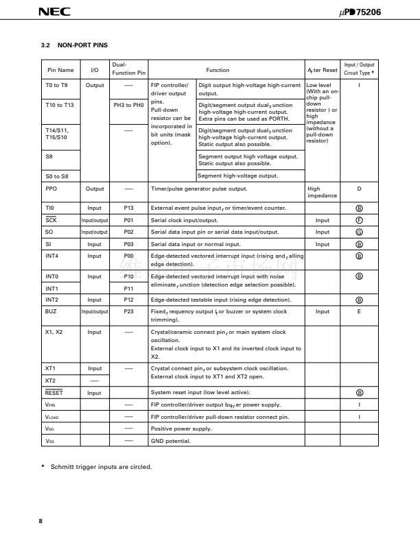
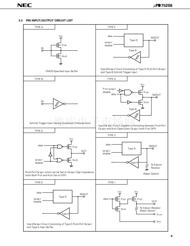
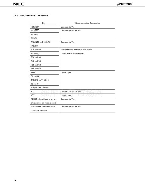
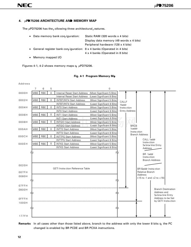
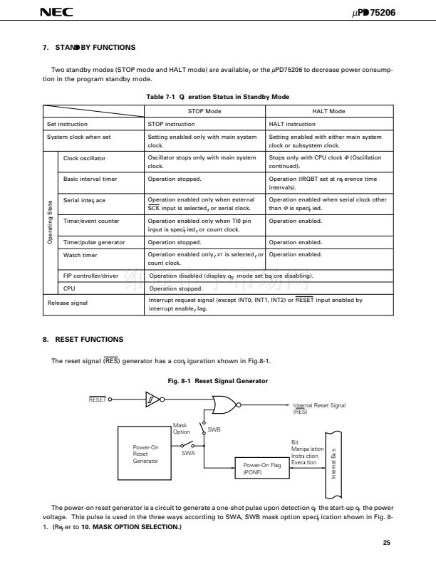
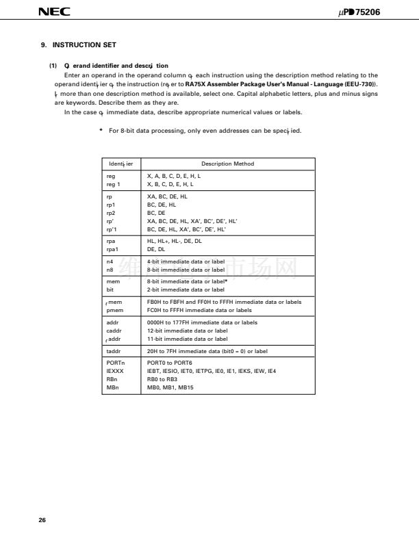
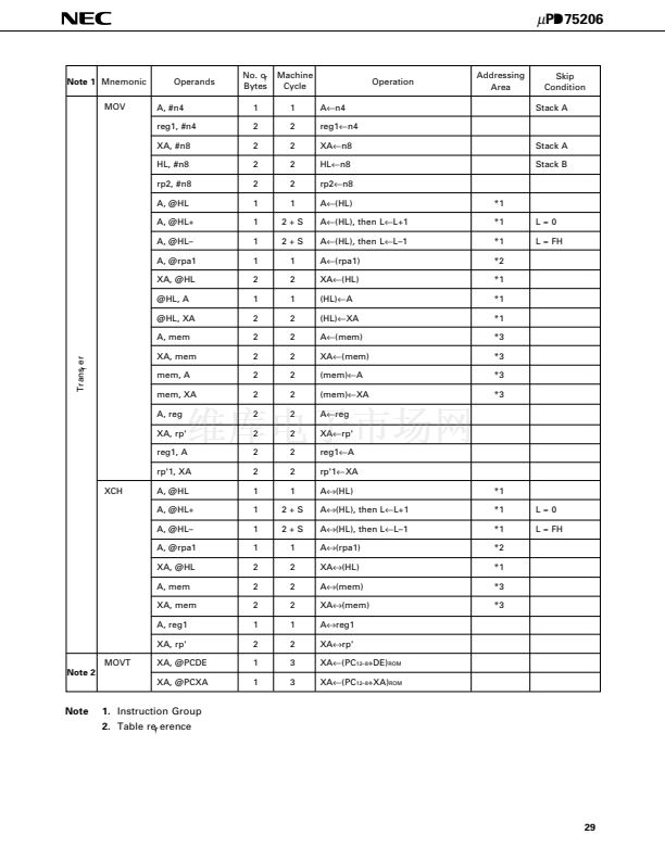
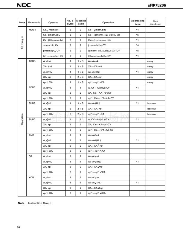
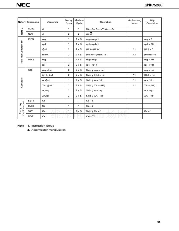
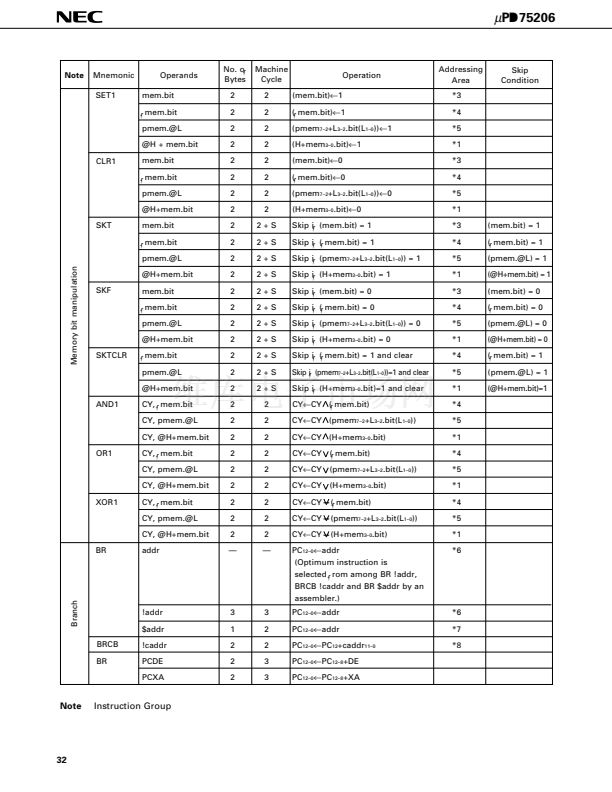
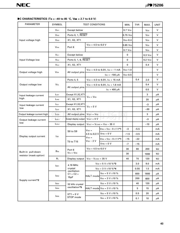
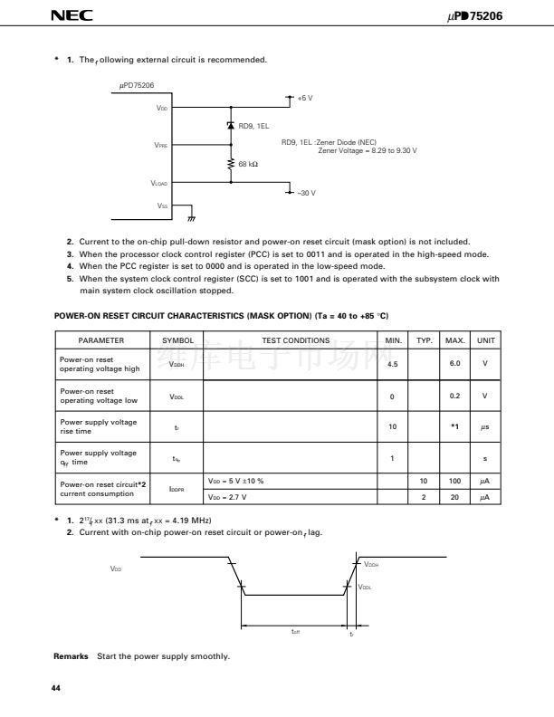
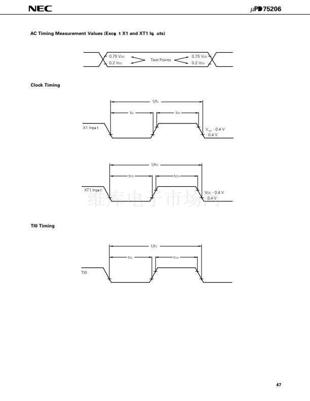
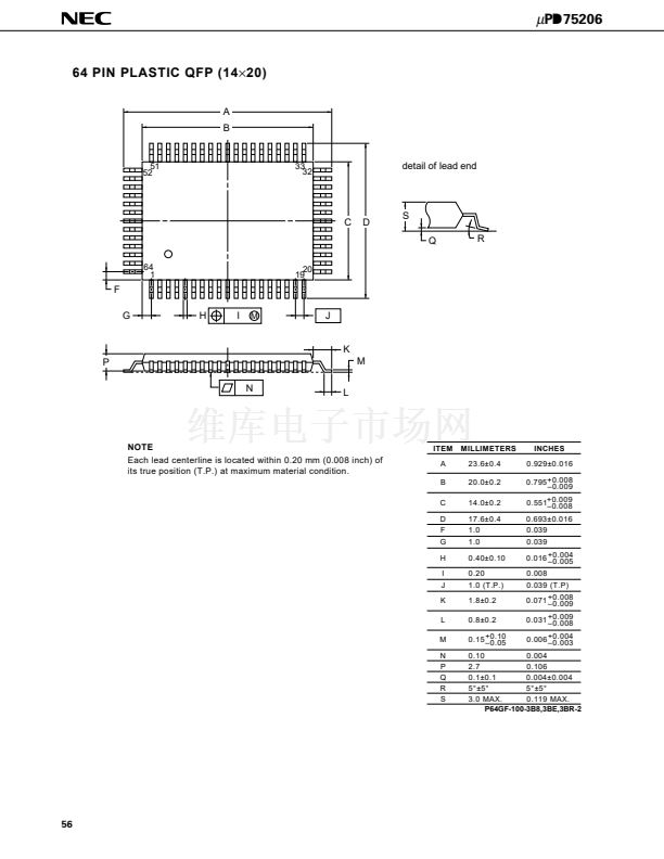
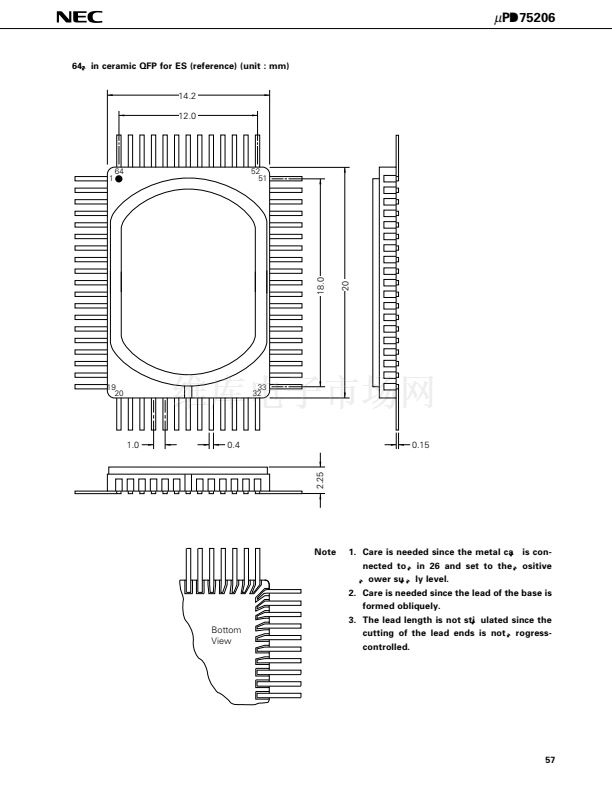
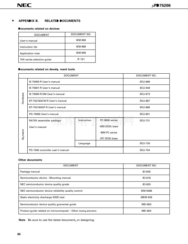
碌
PD75206
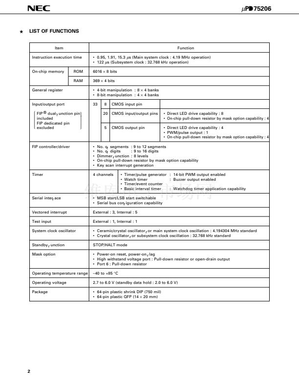
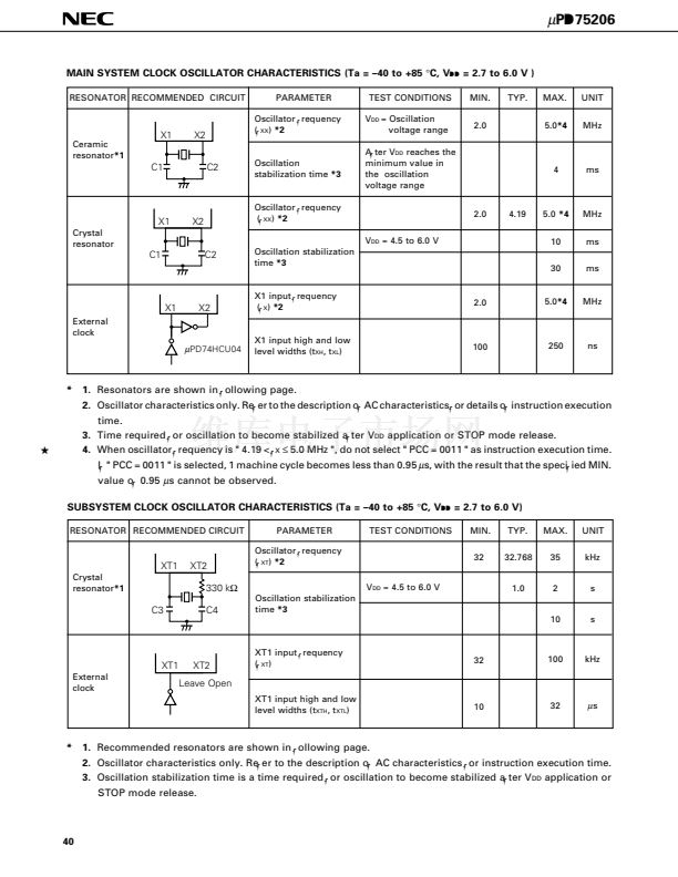
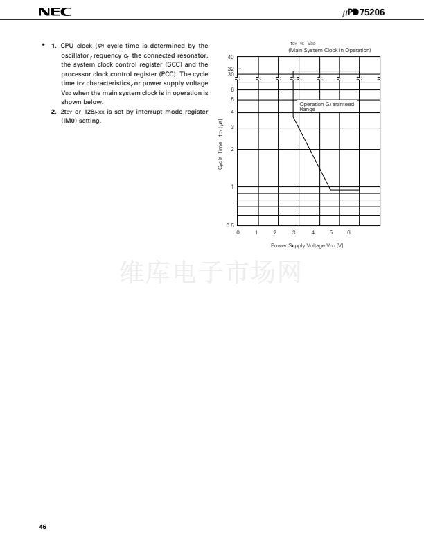
MAIN SYSTEM CLOCK OSCILLATOR CHARACTERISTICS (Ta = 鈥?0 to +85
擄C,
V
DD
= 2.7 to 6.0 V )
RESONATOR RECOMMENDED CIRCUIT
PARAMETER
Oscillator frequency
(f
XX
)
*2
TEST CONDITIONS
V
DD
= Oscillation
voltage range
After V
DD
reaches the
minimum value in
the oscillation
voltage range
2.0
V
DD
= 4.5 to 6.0 V
4.19
MIN.
2.0
TYP.
MAX.
5.0*4
UNIT
MHz
X1
Ceramic
resonator*1
X2
C2
C1
Oscillation
stabilization time
*3
4
ms
X1
Crystal
resonator
X2
C2
Oscillator frequency
(f
XX
)
*2
5.0
*4
10
30
MHz
ms
ms
C1
Oscillation stabilization
time
*3
X1
External
clock
X2
X1 input frequency
(f
X
)
*2
2.0
5.0*4
MHz
碌
PD74HCU04
X1 input high and low
level widths (t
XH
, t
XL
)
100
250
ns
*
1.
Resonators are shown in following page.
2.
Oscillator characteristics only. Refer to the description of AC characteristics for details of instruction execution
time.
3.
Time required for oscillation to become stabilized after V
DD
application or STOP mode release.
4.
When oscillator frequency is " 4.19 < f
X
鈮?/div>
5.0 MHz ", do not select " PCC = 0011 " as instruction execution time.
If " PCC = 0011 " is selected, 1 machine cycle becomes less than 0.95
碌
s, with the result that the specified MIN.
value of 0.95
碌
s cannot be observed.
5
SUBSYSTEM CLOCK OSCILLATOR CHARACTERISTICS (Ta = 鈥?0 to +85
擄C,
V
DD
= 2.7 to 6.0 V)
RESONATOR RECOMMENDED CIRCUIT
PARAMETER
Oscillator frequency
(f
XT
)
*2
V
DD
= 4.5 to 6.0 V
Oscillation stabilization
time
*3
10
s
TEST CONDITIONS
MIN.
32
TYP.
32.768
MAX.
35
UNIT
kHz
XT1
Crystal
resonator*1
XT2
330 k鈩?/div>
1.0
2
s
C3
C4
XT1
External
clock
XT2
Leave Open
XT1 input frequency
(f
XT
)
32
100
kHz
XT1 input high and low
level widths (t
XTH
, t
XTL
)
10
32
碌
s
*
1.
Recommended resonators are shown in following page.
2.
Oscillator characteristics only. Refer to the description of AC characteristics for instruction execution time.
3.
Oscillation stabilization time is a time required for oscillation to become stabilized after V
DD
application or
STOP mode release.
40


 1
1
 2
2
 3
3
 4
4
 5
5
 6
6
 7
7
 8
8
 9
9
 10
10
 11
11
 12
12
 13
13
 14
14
 15
15
 16
16
 17
17
 18
18
 19
19
 20
20
 21
21
 22
22
 23
23
 24
24
 25
25
 26
26
 27
27
 28
28
 29
29
 30
30
 31
31
 32
32
 33
33
 34
34
 35
35
 36
36
 37
37
 38
38
 39
39
 40
40
 41
41
 42
42
 43
43
 44
44
 45
45
 46
46
 47
47
 48
48
 49
49
 50
50
 51
51
 52
52
 53
53
 54
54
 55
55
 56
56
 57
57
 58
58
 59
59
 60
60
 61
61
 62
62
