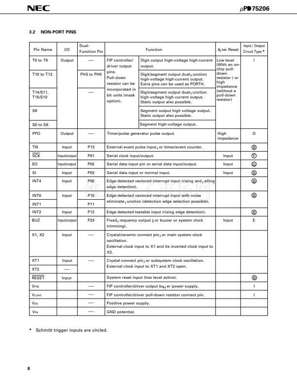
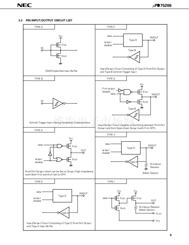
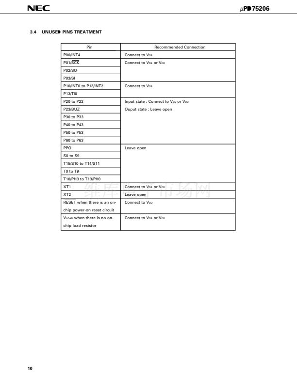
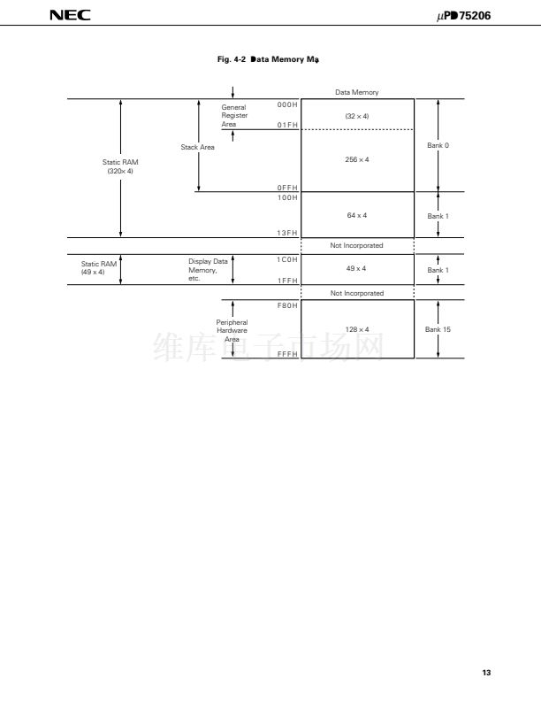
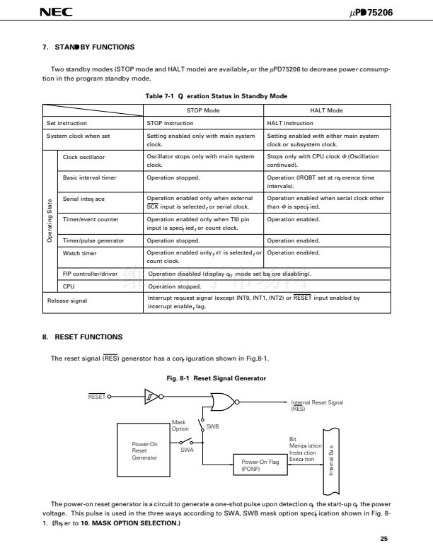
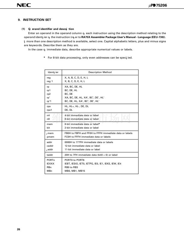
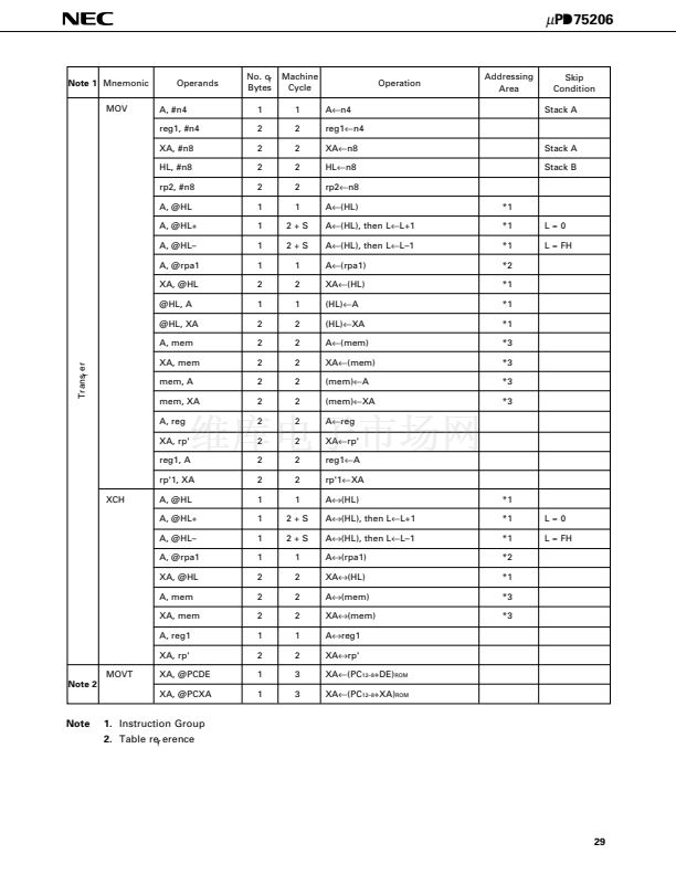
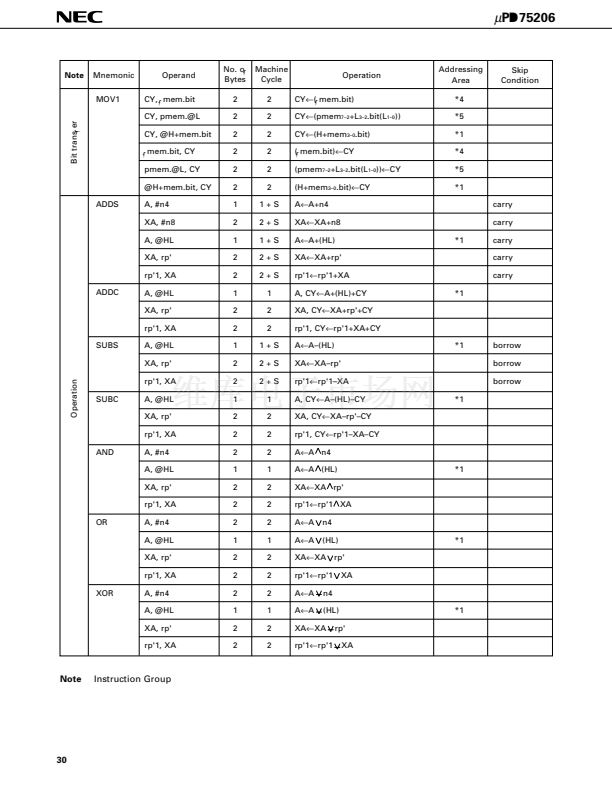
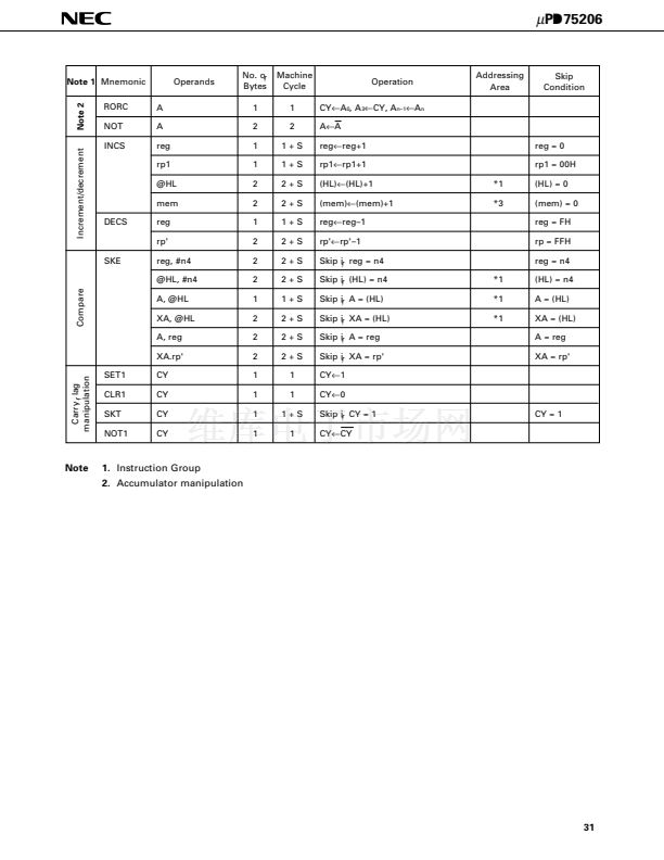
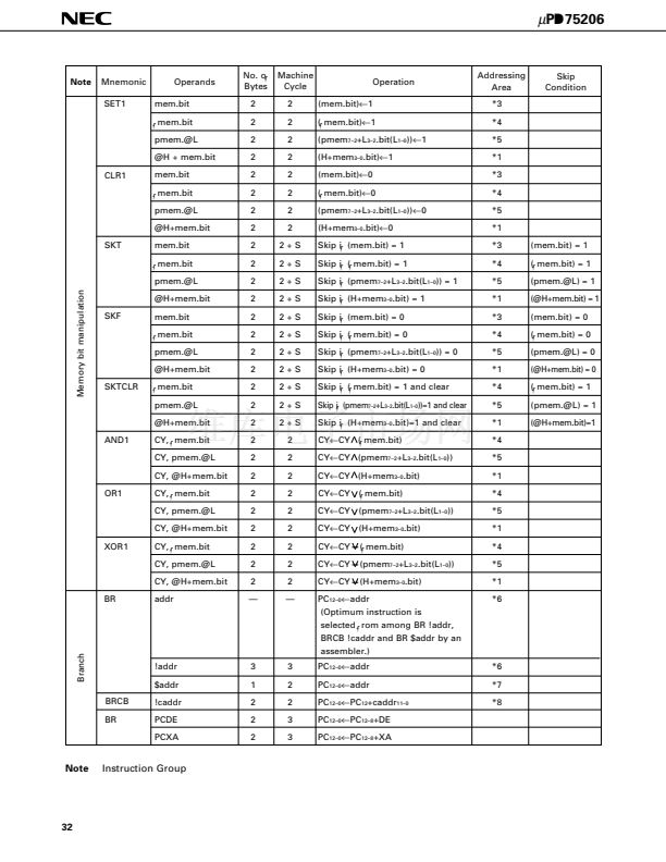
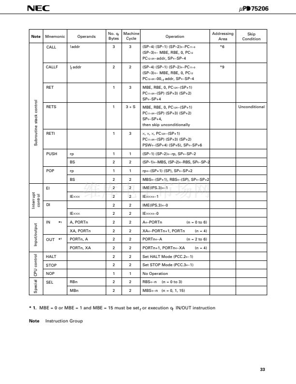
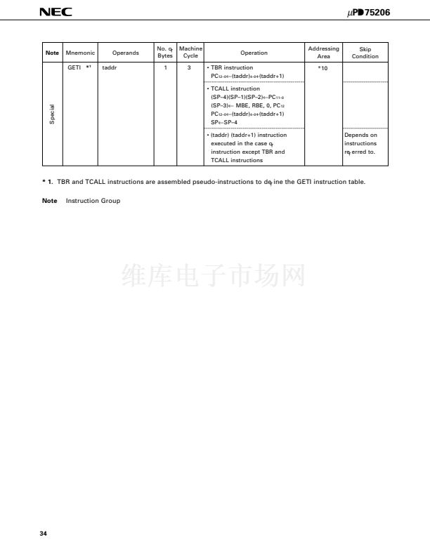
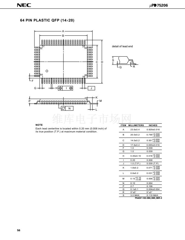
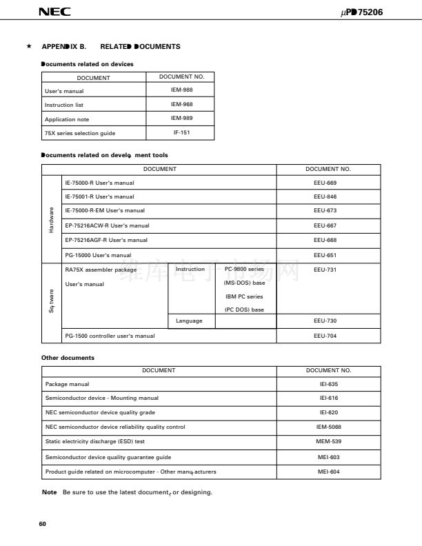
鈥?/div>
122
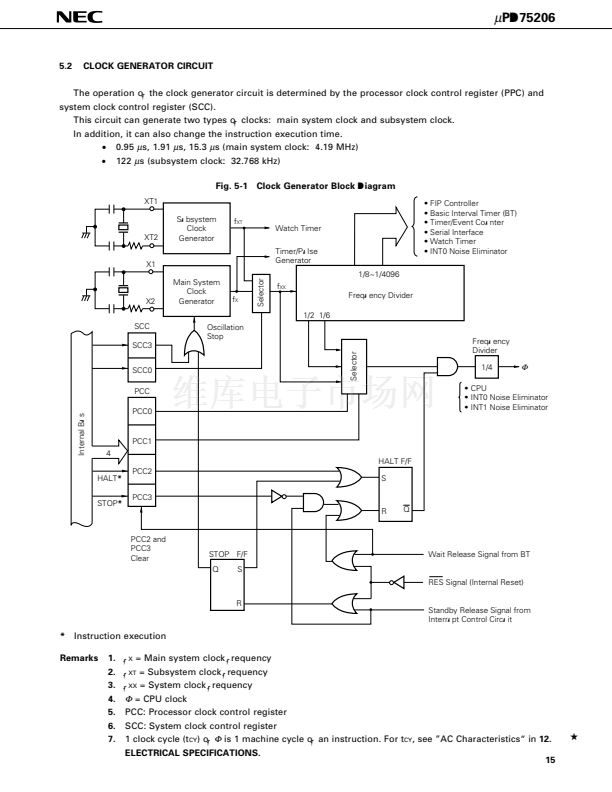
碌
s (subsystem clock: 32.768 kHz)
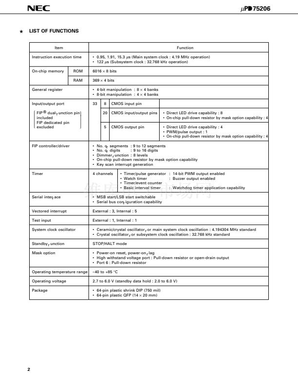
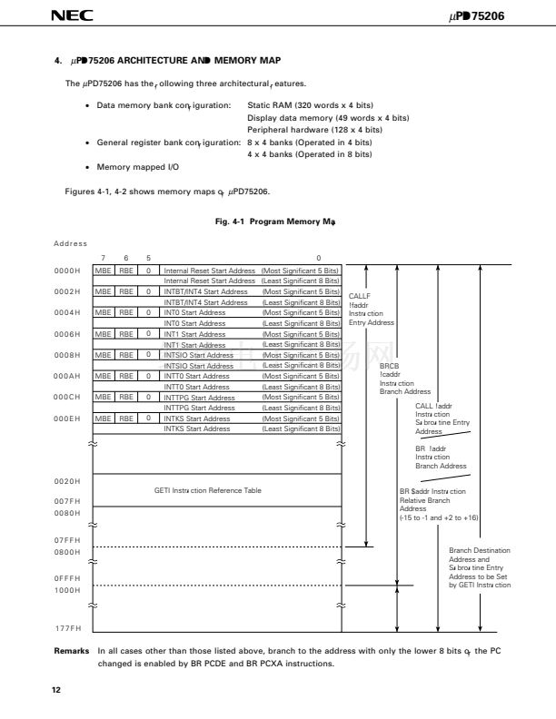
Fig. 5-1 Clock Generator Block Diagram
XT1
Subsystem
Clock
Generator
f
XT
Watch Timer
Timer/Pulse
Generator
Main System
Clock
Generator
Selector
1/8~1/4096
f
XX
Frequency Divider
1/2 1/6
SCC
SCC3
Selector
SCC0
PCC
Internal Bus
PCC0
Oscillation
Stop
Frequency
Divider
1/4
鈥?FIP Controller
鈥?Basic Interval Timer (BT)
鈥?Timer/Event Counter
鈥?Serial Interface
鈥?Watch Timer
鈥?INT0 Noise Eliminator
XT2
X1
X2
f
X
桅
鈥?CPU
鈥?INT0 Noise Eliminator
鈥?INT1 Noise Eliminator
PCC1
4
HALT F/F
HALT*
STOP*
PCC2
PCC3
R
Q
S
PCC2 and
PCC3
Clear
STOP F/F
Q
S
Wait Release Signal from BT
RES Signal (Internal Reset)
R
Standby Release Signal from
Interrupt Control Circuit
*
Instruction execution
1.
2.
3.
4.
5.
6.
7.
f
X
= Main system clock frequency
f
XT
= Subsystem clock frequency
f
XX
= System clock frequency
Remarks
桅
= CPU clock
PCC: Processor clock control register
SCC: System clock control register
1 clock cycle (t
CY
) of
桅
is 1 machine cycle of an instruction. For t
CY
, see 鈥滱C Characteristics鈥?in
12.
ELECTRICAL SPECIFICATIONS.
15
5


 1
1
 2
2
 3
3
 4
4
 5
5
 6
6
 7
7
 8
8
 9
9
 10
10
 11
11
 12
12
 13
13
 14
14
 15
15
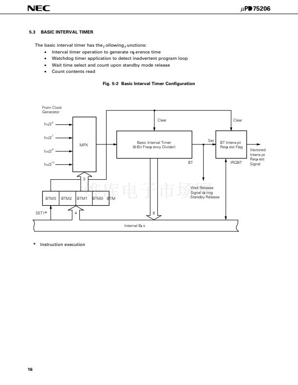 16
16
 17
17
 18
18
 19
19
 20
20
 21
21
 22
22
 23
23
 24
24
 25
25
 26
26
 27
27
 28
28
 29
29
 30
30
 31
31
 32
32
 33
33
 34
34
 35
35
 36
36
 37
37
 38
38
 39
39
 40
40
 41
41
 42
42
 43
43
 44
44
 45
45
 46
46
 47
47
 48
48
 49
49
 50
50
 51
51
 52
52
 53
53
 54
54
 55
55
 56
56
 57
57
 58
58
 59
59
 60
60
 61
61
 62
62
