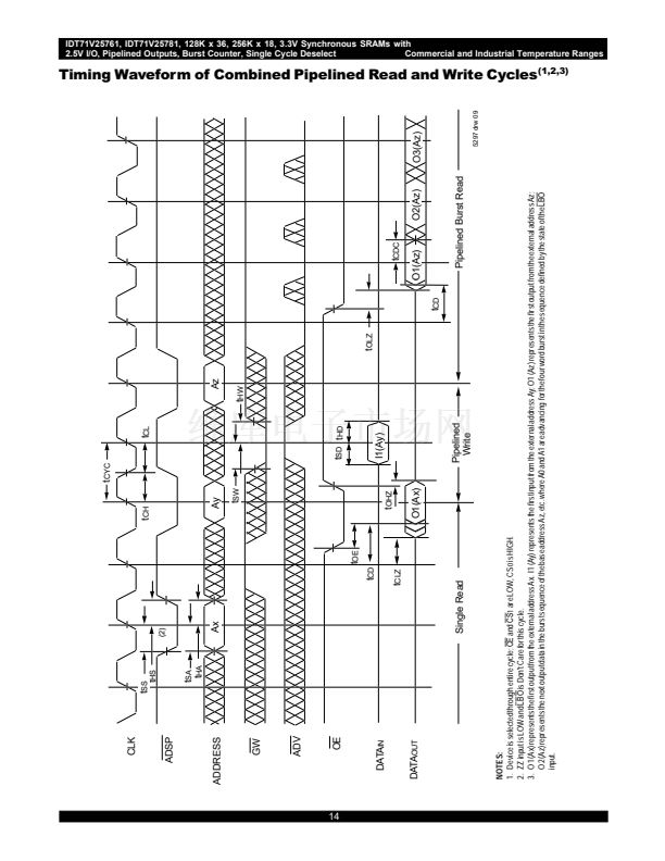
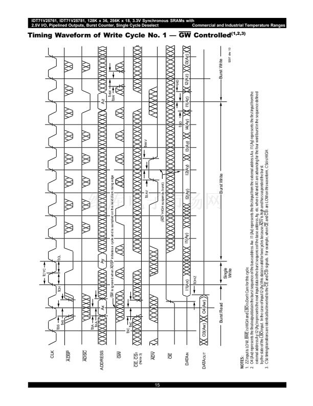
t
CYC
CLK
t
CH
t
CL
t
SS
t
HS
ADSP
ADSC
t
SA
t
HA
Ax
GW
is ignored when
ADSP
initiates a cycle and is sampled on the next clock rising edge
ADDRESS
Ay
Az
t
HW
t
SW
GW
t
SC
t
HC
CE, CS
1
t
SAV
t
HAV
(Note 3)
ADV
(ADV HIGH suspends burst)
Timing Waveform of Write Cycle No. 1 聴
GW
Controlled
(1,2,3)
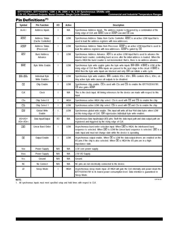
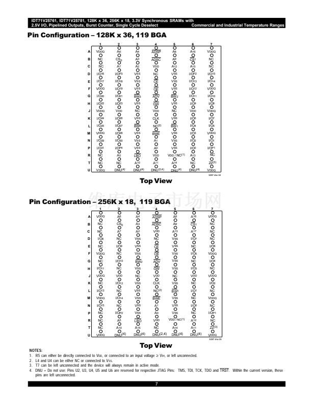
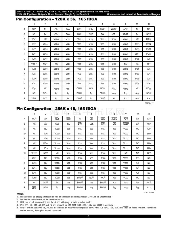
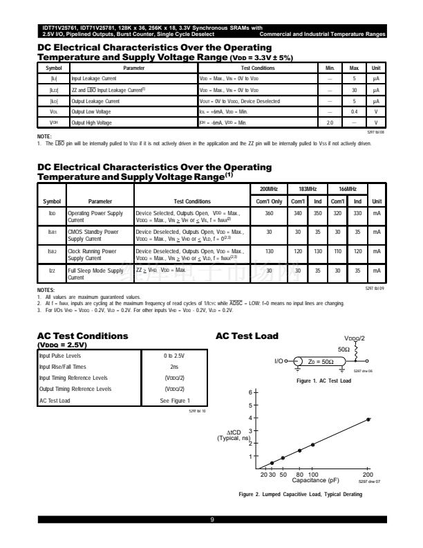
IDT71V25761, IDT71V25781, 128K x 36, 256K x 18, 3.3V Synchronous SRAMs with
2.5V I/O, Pipelined Outputs, Burst Counter, Single Cycle Deselect
Commercial and Industrial Temperature Ranges
6.42
15
I1(Ax)
I2(Ay)
t
OHZ
I1(Ay)
I2(Ay)
Burst Write
Single
Write
OE
t
SD
I3(Ay)
I4(Ay)
I1(Az)
tHD
DATA
IN
I2(Az)
I3(Az)
DATA
OUT
O3(Aw)
O4(Aw)
Burst Read
Burst Write
5297 drw 10
,
NOTES:
1. ZZ input is LOW,
BWE
is HIGH and
LBO
is Don't Care for this cycle.
2. O4 (Aw) represents the final output data in the burst sequence of the base address Aw. I1 (Ax) represents the first input from the external address Ax. I1 (Ay) represents the first input from the
external address Ay; I2 (Ay) represents the next input data in the burst sequence of the base address Ay, etc. where A0 and A1 are advancing for the four word burst in the sequence defined
by the state of the
LBO
input. In the case of input I2 (Ay) this data is valid for two cycles because
ADV
is high and has suspended the burst.
3. CS
0
timing transitions are identical but inverted to the
CE
and
CS
1
signals. For example, when
CE
and
CS
1
are LOW on this waveform, CS
0
is HIGH.
.


 1
1
 2
2
 3
3
 4
4
 5
5
 6
6
 7
7
 8
8
 9
9
 10
10
 11
11
 12
12
 13
13
 14
14
 15
15
 16
16
 17
17
 18
18
 19
19
 20
20
 21
21
 22
22
 23
23
