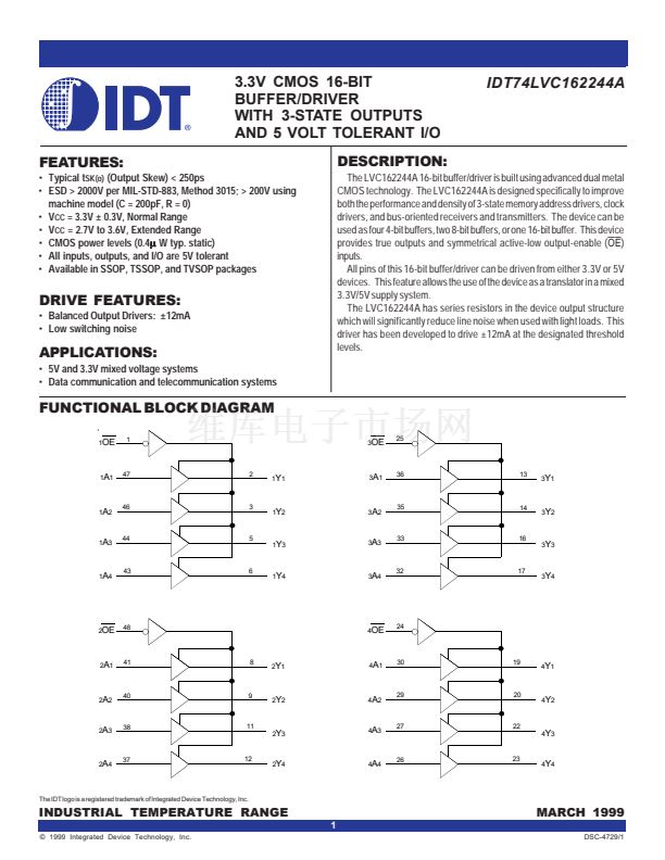
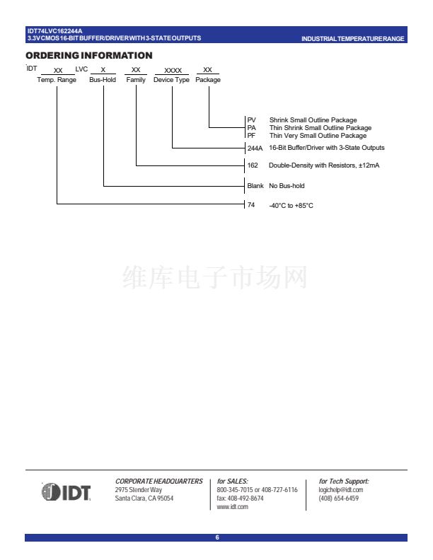
IDT74LVC162244A
3.3V CMOS 16-BIT BUFFER/DRIVER WITH 3-STATE OUTPUTS
INDUSTRIAL TEMPERATURE RANGE
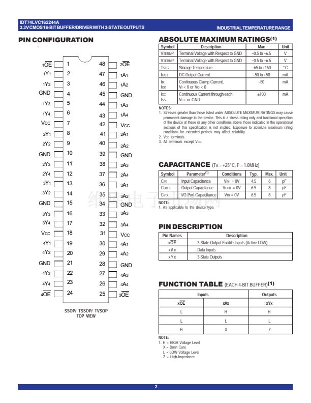
PIN CONFIGURATION
ABSOLUTE MAXIMUM RATINGS
(1)
Symbol
Description
Max
V
TERM
(2)
Terminal Voltage with Respect to GND
鈥?.5 to +6.5
鈥?.5 to +6.5
鈥?5 to +150
鈥?0 to +50
鈥?0
鹵100
V
TERM
(3)
Terminal Voltage with Respect to GND
T
STG
I
OUT
I
IK
I
OK
I
CC
I
SS
Storage Temperature
DC Output Current
Continuous Clamp Current,
V
I
< 0 or V
O
< 0
Continuous Current through each
V
CC
or GND
Unit
V
V
擄C
mA
mA
mA
1
OE
1
Y
1
1
Y
2
1
2
3
4
5
6
7
8
9
10
11
12
13
14
15
16
17
18
19
20
21
22
23
24
48
47
46
45
44
43
42
41
40
39
38
37
36
35
34
33
32
31
30
29
28
27
26
25
2
OE
1
A
1
1
A
2
GND
1
Y
3
1
Y
4
GND
1
A
3
1
A
4
V
CC
2
Y
1
2
Y
2
V
CC
2
A
1
2
A
2
NOTES:
1. Stresses greater than those listed under ABSOLUTE MAXIMUM RATINGS may cause
permanent damage to the device. This is a stress rating only and functional operation
of the device at these or any other conditions above those indicated in the operational
sections of this specification is not implied. Exposure to absolute maximum rating
conditions for extended periods may affect reliability.
2. V
CC
terminals.
3. All terminals except V
CC
.
GND
2
Y
3
2
Y
4
3
Y
1
3
Y
2
GND
2
A
3
2
A
4
3
A
1
3
A
2
CAPACITANCE
(T
A
= +25擄C, F = 1.0MHz)
Symbol
C
IN
C
OUT
C
I/O
Parameter
(1)
Input Capacitance
Output Capacitance
I/O Port Capacitance
Conditions
V
IN
= 0V
V
OUT
= 0V
V
IN
= 0V
Typ.
4.5
6.5
6.5
Max.
6
8
8
Unit
pF
pF
pF
GND
3
Y
3
3
Y
4
GND
3
A
3
3
A
4
NOTE:
1. As applicable to the device type.
PIN DESCRIPTION
Pin Names
xOE
xAx
xYx
Data Inputs
3-State Outputs
Description
3-State Output Enable Inputs (Active LOW)
V
CC
4
Y
1
4
Y
2
V
CC
4
A
1
4
A
2
GND
4
Y
3
4
Y
4
4
OE
GND
4
A
3
4
A
4
3
OE
FUNCTION TABLE
(EACH 4-BIT BUFFER)
(1)
Inputs
xOE
xAx
H
L
X
Outputs
xYx
H
L
Z
SSOP/ TSSOP/ TVSOP
TOP VIEW
L
L
H
NOTE:
1. H = HIGH Voltage Level
X = Don鈥檛 Care
L = LOW Voltage Level
Z = High-Impedance
2


 1
1
 2
2
 3
3
 4
4
 5
5
 6
6
