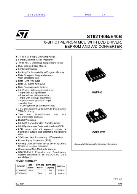
ST62T40B/E40B
6.3 DC ELECTRICAL CHARACTERISTICS
(T
A
= -40 to +85擄C unless otherwise specified)
Symbol
Parameter
Test Conditions
Value
Min.
Typ.
Max.
Unit
V
IL
V
IH
V
Hys
V
OL
V
OH
R
PU
I
IL
I
IH
I
DD
V
DD
= 5V
V
DD
= 3V
V
DD
= 5.0V; I
OL
= +10碌A(chǔ)
V
DD
= 5.0V; I
OL
= + 5mA
V
DD
= 5.0V; I
OL
= +10碌A(chǔ)
Low Level Output Voltage
V
DD
= 5.0V; I
OL
= +10mA
20 mA Sink I/O pins
V
DD
= 5.0V; I
OL
= +20mA
High Level Output Voltage V
DD
= 5.0V; I
OL
= -10碌A(chǔ)
All Output pins
V
DD
= 5.0V; I
OL
= -5.0mA
All Input pins
Pull-up Resistance
RESET pin
Input Leakage Current
V
IN
= V
SS
(No Pull-Up configured)
All Input pins but RESET V
IN
= V
DD
Input Leakage Current
V
IN
= V
SS
RESET pin
V
IN
= V
DD
Supply Current in RESET V
RESET
=V
SS
f
OSC
=8MHz
Mode
Supply Current in
V
DD
=5.0V f
INT
=8MHz
RUN Mode
(2)
Supply Current in WAIT
V
DD
=5.0V f
INT
=8MHz
Mode
(3)
Supply Current in STOP
I
LOAD
=0mA
Mode
(3)
V
DD
=5.0V
Input Low Level Voltage
All Input pins
Input High Level Voltage
All Input pins
Hysteresis Voltage
(1)
All Input pins
Low Level Output Voltage
All Output pins
V
DD
x 0.3
V
DD
x 0.7
0.2
0.2
0.1
0.8
0.1
0.8
1.3
4.9
3.5
40
150
V
V
V
V
V
100
350
0.1
200
900
1.0
-30
10
7
7
2
10
碌A(chǔ)
螝鈩?/div>
-8
-16
mA
mA
mA
碌A(chǔ)
Notes:
(1) Hysteresis voltage between switching levels
(2) All peripherals running
(3) All peripherals in stand-by
63/76
635


 1
1
 2
2
 3
3
 4
4
 5
5
 6
6
 7
7
 8
8
 9
9
 10
10
 11
11
 12
12
 13
13
 14
14
 15
15
 16
16
 17
17
 18
18
 19
19
 20
20
 21
21
 22
22
 23
23
 24
24
 25
25
 26
26
 27
27
 28
28
 29
29
 30
30
 31
31
 32
32
 33
33
 34
34
 35
35
 36
36
 37
37
 38
38
 39
39
 40
40
 41
41
 42
42
 43
43
 44
44
 45
45
 46
46
 47
47
 48
48
 49
49
 50
50
 51
51
 52
52
 53
53
 54
54
 55
55
 56
56
 57
57
 58
58
 59
59
 60
60
 61
61
 62
62
 63
63
 64
64
 65
65
 66
66
 67
67
 68
68
 69
69
 70
70
 71
71
 72
72
 73
73
 74
74
 75
75
 76
76
