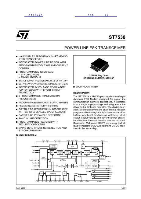
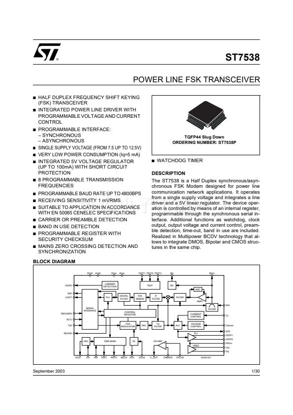
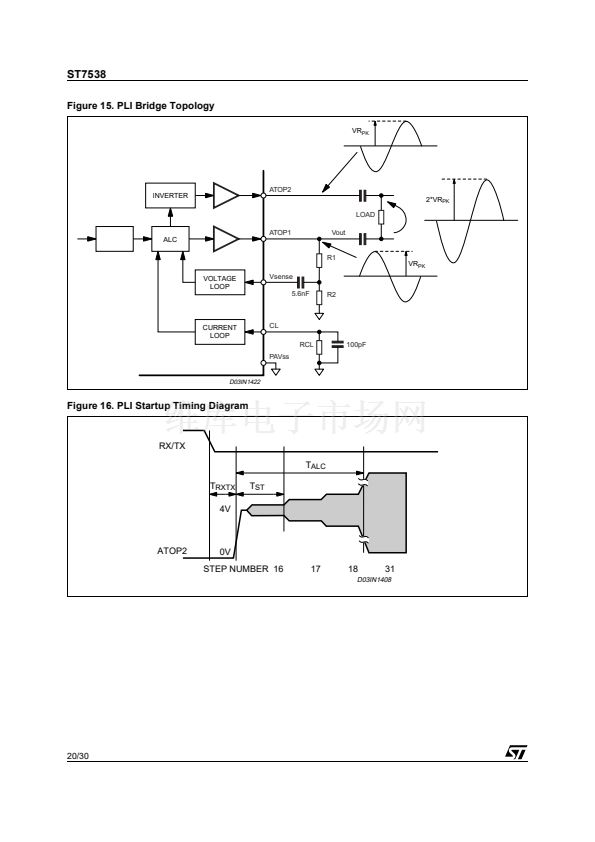
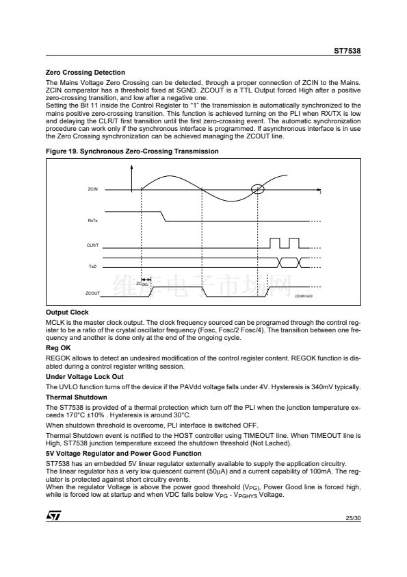
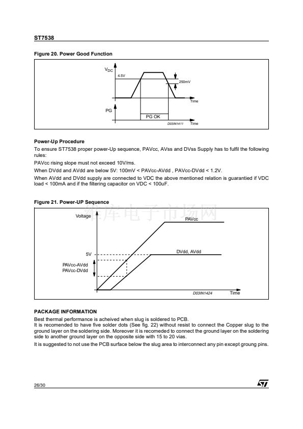
ST7538
ABSOLUTE MAXIMUM RATINGS
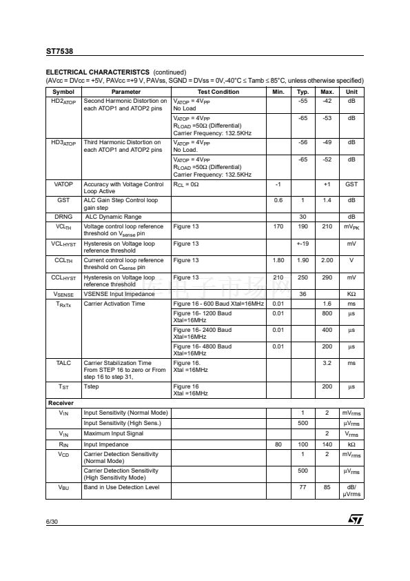
Symbol
PAV
CC
AV
dd
DV
dd
AV
ss
/DV
ss
V
I
V
O
I
O
V
sense
RAI
ATO
ATO
ATOP1,2
ATOP
T
amb
T
stg
ATOP1 Pin
ATOP2 Pin
Other pins
Power Supply Voltage
Analog Supply Voltage
Digital Supply Voltage
Voltage between AV
ss
and DV
ss
Digital input Voltage
Digital output Voltage
Digital Output Current
Voltage Range at Vsense Input
Voltage Range at RAI Input
Output Current at ATO Output
Voltage range at ATO Output
Voltage range at Powered ATO Output
Powered ATO Output Current
Operating ambient Temperature
Storage Temperature
Maximum Withstanding Voltage Range
Test Condition: CDF-AEC-Q100-002- 鈥淗uman Body Model鈥?/div>
Acceptance Criteria: 鈥淣ormal Performance鈥?/div>
Parameter
Value
-0.3 to +14
-0.3 to +5.5
-0.3 to +5.5
-0.3 to +0.3
DV
ss
- 0.3 to DV
dd
+0.3
DV
ss
- 0.3 to DV
dd
+0.3
-2 to +2
AV
ss
- 0.3 to AV
dd
+0.3
-AV
dd
- 0.3 to AV
dd
+0.3
-2 to +2
AV
ss
- 0.3 to AV
dd
+0.3
AV
ss
- 0.3 to +PAV
cc
+0.3
400
-40 to +85
-50 to 150
鹵1500
鹵1000
鹵2000
Unit
V
V
V
V
V
V
mA
V
V
mA
V
V
mARms
擄C
擄C
V
V
V
THERMAL DATA
Symbol
R
th-j-amb1
R
th-j-amb2
Parameter
Maximum Thermal Resistance Junction-Ambient Steady State(*)
Maximum Thermal Resistance Junction-Ambient Steady State(**)
TQFP44
with slug
35
50
Unit
擄C/W
擄C/W
(*) Mounted on Multilayer PCB with a dissipating surface on the bottom side of the PCB
(**) It's the same condition of the point above, without any heatsinking surface on the board.
4/30


 1
1
 2
2
 3
3
 4
4
 5
5
 6
6
 7
7
 8
8
 9
9
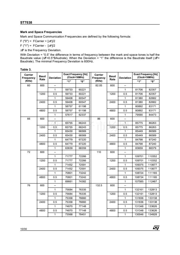 10
10
 11
11
 12
12
 13
13
 14
14
 15
15
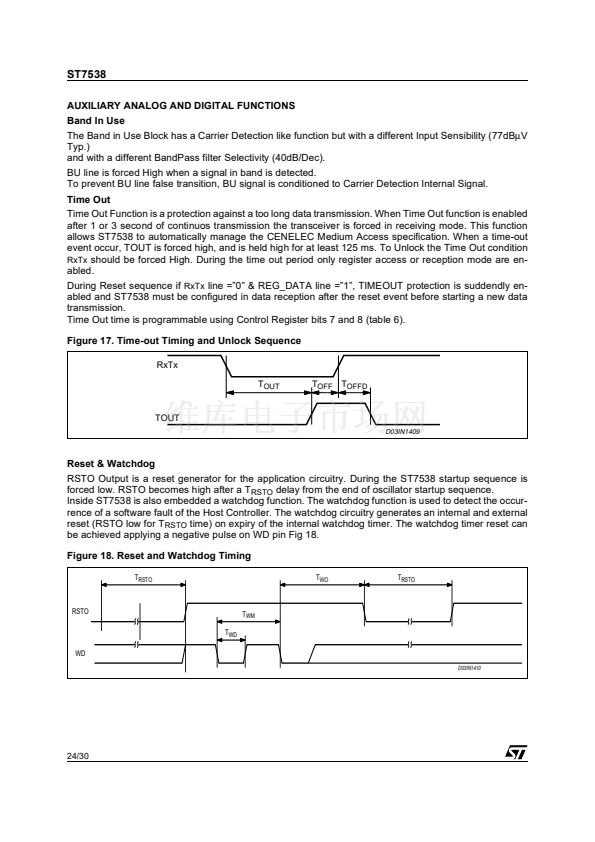
 16
16
 17
17
 18
18
 19
19
 20
20
 21
21
 22
22
 23
23
 24
24
 25
25
 26
26
 27
27
 28
28
 29
29
 30
30
