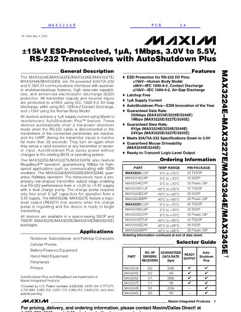
鈥?/div>
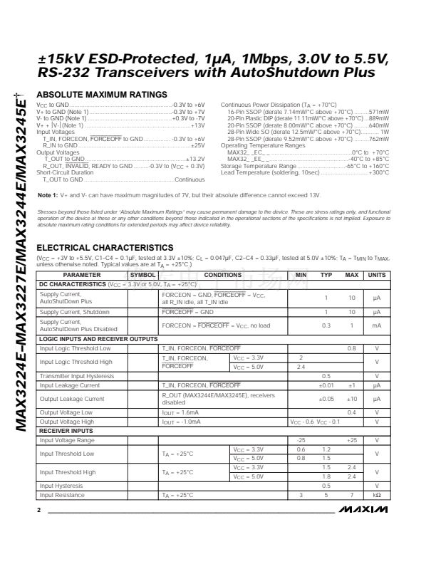
ABSOLUTE MAXIMUM RATINGS
V
CC
to GND ..............................................................-0.3V to +6V
V+ to GND (Note 1) ..................................................-0.3V to +7V
V- to GND (Note 1) ...................................................+0.3V to -7V
V+ +
錚-錚?Note
1) ................................................................+13V
Input Voltages
T_IN, FORCEON,
FORCEOFF
to GND ................ -0.3V to +6V
R_IN to GND ....................................................................鹵25V
Output Voltages
T_OUT to GND.............................................................鹵13.2V
R_OUT,
INVALID,
READY to GND .........-0.3V to (V
CC
+ 0.3V)
Short-Circuit Duration
T_OUT to GND .......................................................Continuous
Continuous Power Dissipation (T
A
= +70擄C)
16-Pin SSOP (derate 7.14mW/擄C above +70擄C) .........571mW
20-Pin Plastic DIP (derate 11.11mW/擄C above +70擄C) ...889mW
20-Pin SSOP (derate 8.00mW/擄C above +70擄C) .........640mW
28-Pin Wide SO (derate 12.5mW/擄C above +70擄C)........... 1W
28-Pin SSOP (derate 9.52mW/擄C above +70擄C) .........762mW
Operating Temperature Ranges
MAX32_ _EC_ _ .................................................0擄C to +70擄C
MAX32_ _EE_ _................................................-40擄C to +85擄C
Storage Temperature Range .............................-65擄C to +160擄C
Lead Temperature (soldering, 10sec) .............................+300擄C
Note 1:
V+ and V- can have maximum magnitudes of 7V, but their absolute difference cannot exceed 13V.
Stresses beyond those listed under 鈥淎bsolute Maximum Ratings鈥?may cause permanent damage to the device. These are stress ratings only, and functional
operation of the device at these or any other conditions beyond those indicated in the operational sections of the specifications is not implied. Exposure to
absolute maximum rating conditions for extended periods may affect device reliability.
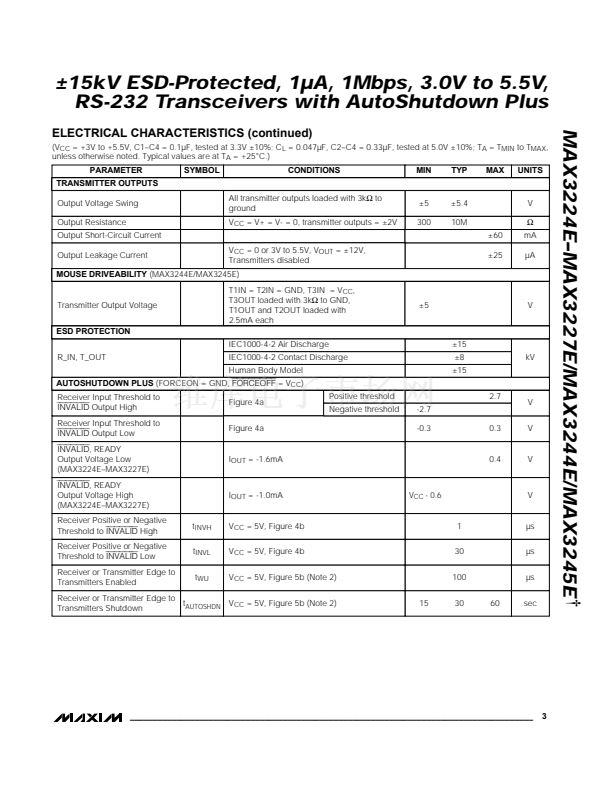
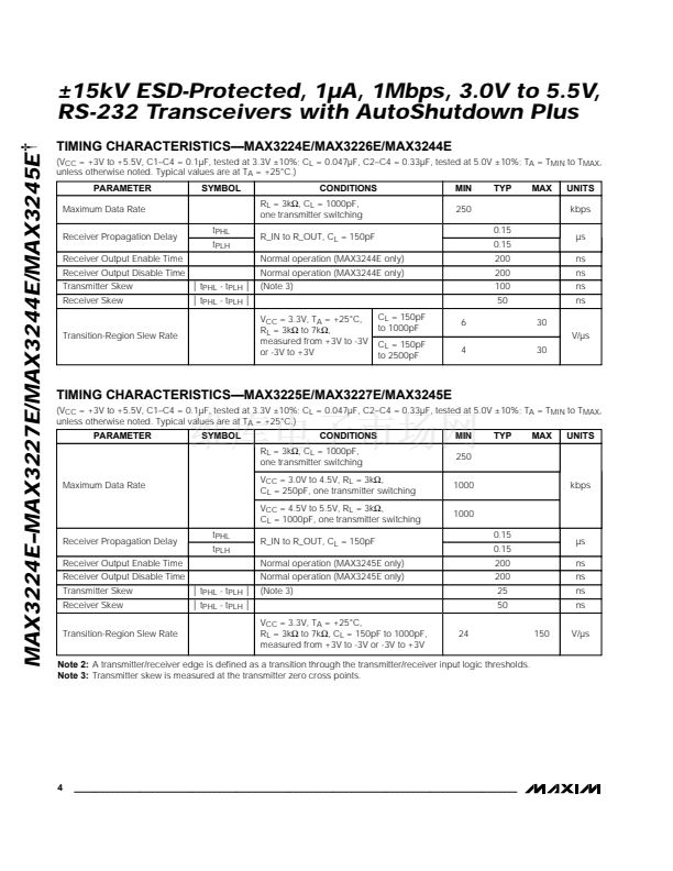
ELECTRICAL CHARACTERISTICS
(V
CC
= +3V to +5.5V, C1鈥揅4 = 0.1碌F, tested at 3.3V 鹵10%; C
L
= 0.047碌F, C2鈥揅4 = 0.33碌F, tested at 5.0V 鹵10%; T
A
= T
MIN
to T
MAX
,
unless otherwise noted. Typical values are at T
A
= +25擄C.)
PARAMETER
Supply Current,
AutoShutDown Plus
Supply Current, Shutdown
Supply Current,
AutoShutDown Plus Disabled
LOGIC INPUTS AND RECEIVER OUTPUTS
Input Logic Threshold Low
Input Logic Threshold High
Transmitter Input Hysteresis
Input Leakage Current
Output Leakage Current
Output Voltage Low
Output Voltage High
RECEIVER INPUTS
Input Voltage Range
Input Threshold Low
Input Threshold High
Input Hysteresis
Input Resistance
2
T
A
= +25擄C
3
T
A
= +25擄C
T
A
= +25擄C
V
CC
= 3.3V
V
CC
= 5.0V
V
CC
= 3.3V
V
CC
= 5.0V
-25
0.6
0.8
1.2
1.5
1.5
1.8
0.5
5
7
2.4
2.4
+25
V
V
V
V
k鈩?/div>
T_IN, FORCEON,
FORCEOFF
R_OUT (MAX3244E/MAX3245E), receivers
disabled
I
OUT
= 1.6mA
I
OUT
= -1.0mA
V
CC
- 0.6 V
CC
- 0.1
T_IN, FORCEON,
FORCEOFF
T_IN, FORCEON,
FORCEOFF
V
CC
= 3.3V
V
CC
= 5.0V
2
2.4
0.5
鹵0.01
鹵0.05
鹵1
鹵10
0.4
0.8
V
V
V
碌A(chǔ)
碌A(chǔ)
V
V
SYMBOL
CONDITIONS
FORCEON = GND,
FORCEOFF
= V
CC
,
all R_IN idle, all T_IN idle
FORCEOFF
= GND
FORCEON =
FORCEOFF
= V
CC
, no load
MIN
TYP
MAX
UNITS
DC CHARACTERISTICS
(V
CC
= 3.3V or 5.0V, T
A
= +25擄C)
1
1
0.3
10
10
1
碌A(chǔ)
碌A(chǔ)
mA
_______________________________________________________________________________________


 1
1
 2
2
 3
3
 4
4
 5
5
 6
6
 7
7
 8
8
 9
9
 10
10
 11
11
 12
12
 13
13
 14
14
 15
15
 16
16
 17
17
 18
18
 19
19
 20
20
