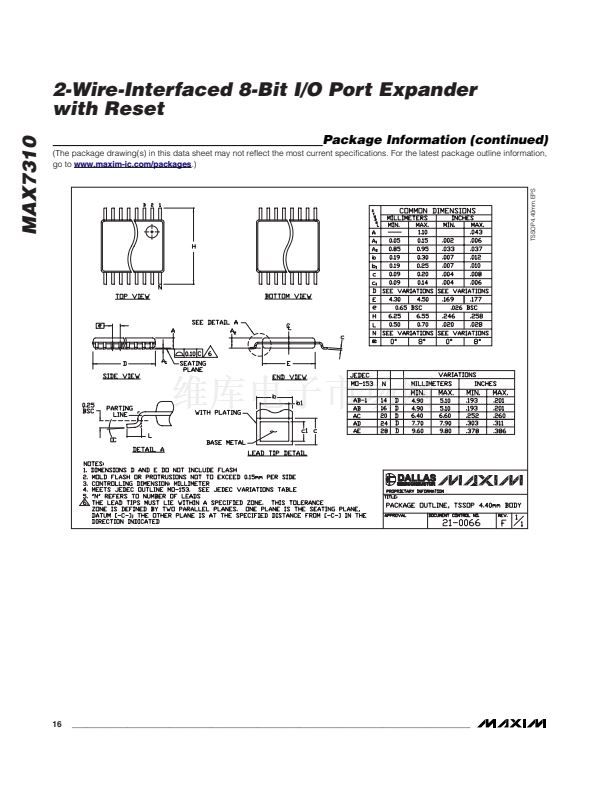
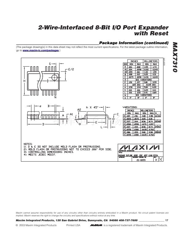
2-Wire-Interfaced 8-Bit I/O Port Expander
with Reset
MAX7310
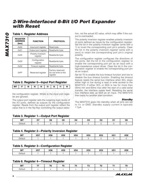
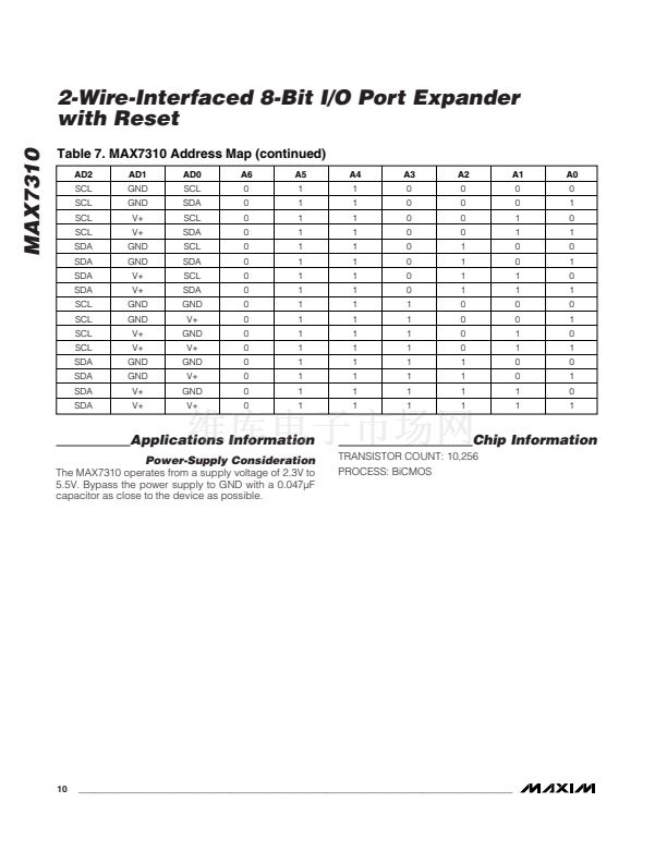
Table 1. Register Address
REGISTER
ADDRESS
(hex)
0x00
0x01
0x02
0x03
0x04
0xFF
FUNCTION
Input port register
Output port register
Polarity inversion
register
Configuration
register
Timeout register
Reserved register
PROTOCOL
Read byte.
Read/write byte.
Read/write byte.
Read/write byte.
Read/write byte.
Factory reserved.
Do not write to this
register.
tion, not the actual I/O value, which may differ if the out-
put is overloaded.
The polarity inversion register enables polarity inversion
of ports defined as inputs by the configuration register.
Set the bit in the polarity inversion register (write with a
1) to invert the corresponding port pin鈥檚 polarity. Clear
the bit in the polarity inversion register (write with a
zero) to retain the corresponding port pin鈥檚 original
polarity.
The configuration register configures the directions of
the ports. Set the bit in the configuration register to
enable the corresponding port pin as an input with a
high-impedance output driver. Clear the bit in the con-
figuration register to enable the corresponding port pin
as an output.
Set bit T0 to enable the bus timeout function and low to
disable the bus timeout function. Enabling the timeout
feature resets the serial bus interface when SCL stops
either high or low during a read or write access to the
MAX7310. If either SCL or SDA is low for more than
30ms min and 60ms max after the start of a valid serial
transfer, the interface resets itself. Resetting the serial
bus interface sets up SDA as an input. The MAX7310
then waits for another start condition.
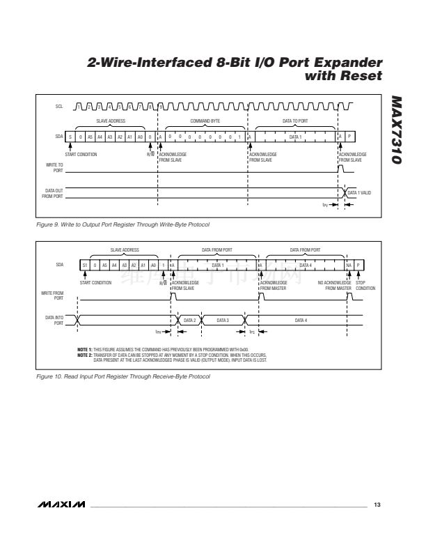
Table 2. Register 0鈥擨nput Port Register
BIT
I7
I6
I5
I4
I3
I2
I1
I0
the configuration register. Writes to the input port regis-
ter are ignored.
The output port register sets the outgoing logic levels of
the I/O ports, defined as outputs by the configuration
register. Reads from the output port register reflect the
value that is in the flip-flop controlling the output selec-
Standby
The MAX7310 goes into standby when all pins are set
to V+ or GND. Standby supply current is typically
1.7碌A(chǔ).
Table 3. Register 1鈥擮utput Port Register
BIT
Default
O7
0
O6
0
O5
0
O4
0
O3
0
O2
0
O1
0
O0
0
Table 4. Register 2鈥擯olarity Inversion Register
BIT
Default
I/O7
1
I/O6
1
I/O5
1
I/O4
1
I/O3
0
I/O2
0
I/O1
0
I/O0
0
Table 5. Register 3鈥擟onfiguration Register
BIT
Default
I/O7
1
I/O6
1
I/O5
1
I/O4
1
I/O3
1
I/O2
1
I/O1
1
I/O0
1
Table 6. Register 4鈥擳imeout Register
BIT
Default
T7
x
T6
x
T5
x
T4
x
T3
x
T2
x
T1
x
T0
1
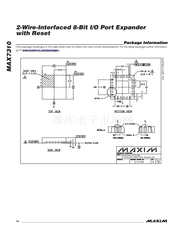
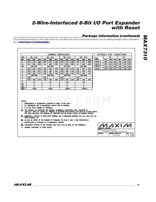
8
_______________________________________________________________________________________


 1
1
 2
2
 3
3
 4
4
 5
5
 6
6
 7
7
 8
8
 9
9
 10
10
 11
11
 12
12
 13
13
 14
14
 15
15
 16
16
 17
17
