2SK2919
Continued from preceding page.
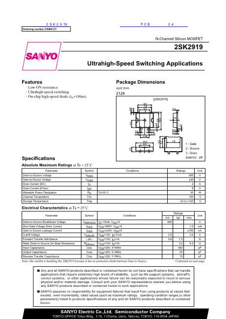
Parameter
Turn-ON Delay Time
Rise Time
Turn-OFF Delay Time
Fall Time
Diode Forward Voltage
Diode Reverse recovery time
Symbol
td(on)
tr
td(off)
tf
VSD
trr
Conditions
See specified Test Circuit
See specified Test Circuit
See specified Test Circuit
See specified Test Circuit
IS=2A, VGS=0
IS=2A, di/dt=100A碌s
100
Ratings
min
typ
10
12
65
40
1.5
max
Unit
ns
ns
ns
ns
V
ns
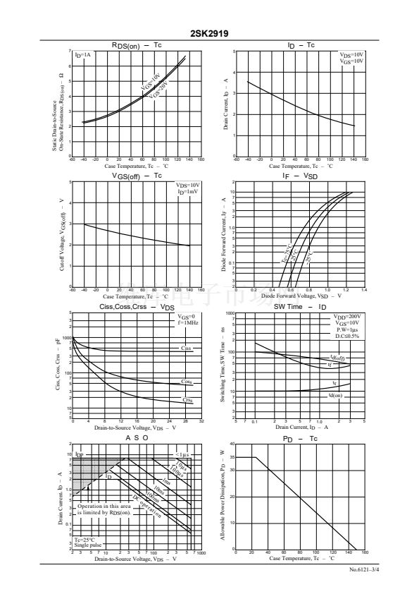
Switching Time Test Circuit
10V
0V
VGS
VDD=200V
ID=1A
RL=200鈩?/div>
D
VOUT
VGS
PW=1碌s
D.C.鈮?.5%
G
2SK2919
P.G
50鈩?/div>
S
5
I D - VDS
3.6
3.2
ID - VGS
VDS=10V
Tc=-25擄C
25擄C
4
6.0V
5.5V
2.8
Drain Current, I
D
鈥?A
Drain Current, I
D
鈥?A
10V
3
2.4
75擄C
2.0
1.6
1.2
0.8
5.0V
2
4.5V
1
4.0V
VGS=3.5V
0
0
4
8
12
16
20
0.4
0
0
2
4
6
8
10
12
14
Drain-to-Source Voltage, V
DS
鈥?V
Gate-to-Source Voltage, V
GS
鈥?V
6
| y
f s
| - I
D
5
R DS(on) - VGS
Tc=25擄C
Forward Transfer Admittance, | yfs | 鈥?S
VDS=10V
3
1.0
7
5
3
2
5
擄
C
=-2
Tc
C
75
擄
C
25
擄
Static Drain-to-Source
On-State Resistance, R
DS (on)
鈥?/div>
鈩?/div>
2
5
4
ID=2A
1A
3
0.5A
2
0.1
7
5
5
7
0.1
2
3
5
7 1.0
2
3
5
7
10
1
0
0
2
4
6
8
10
12
14
Drain Current, I
D
鈥?A
Gate-to-Source Voltage, V
GS
鈥?V
No.6121鈥?/4


 1
1
 2
2
 3
3
 4
4
