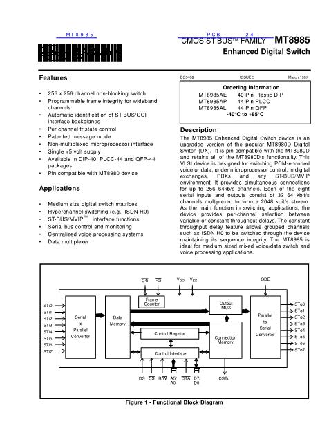
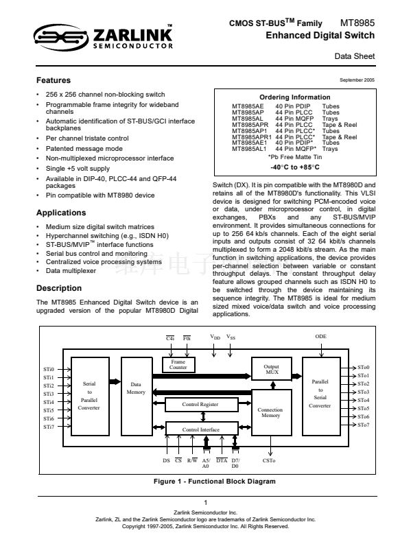
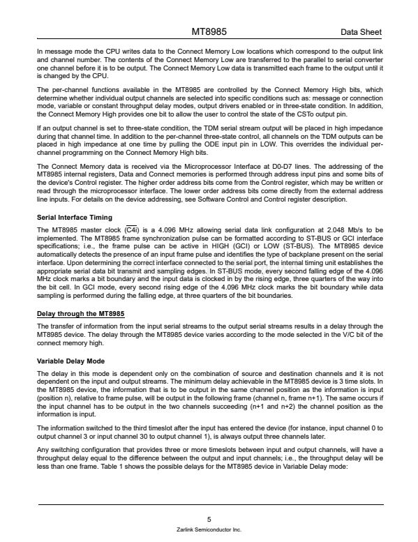
MT8985
Input
Channel
n
n
Output Channel
m=n, n+1 or n+2
m>n+2
Throughput Delay
m-n + 32 timeslots
m-n time slots
Data Sheet
n
m<n
32-(n-m) time slots
Table 1 - Channel Delay for the Variable Mode Delay
Constant Delay Mode
In this mode frame integrity is maintained in all switching configurations by making use of a multiple Data-Memory
buffer technique where input channels written in any of the buffers during frame N will be read out during frame
N+2. In the MT8985, the minimum throughput delay achievable in Constant Delay mode will be 32 time slots; for
example, when input time slot 32 (channel 31) is switched to output time slot 1 (channel 0). Likewise, the maximum
delay is achieved when the first time slot in a frame (channel 0) is switched to the last time slot in the frame
(channel 31), resulting in 94 time slots of delay.
To summarize, any input time slot from input frame N will be always switched to the destination time slot on output
frame N+2. In Constant Delay mode, the device throughput delay is calculated according to the following formula:
DELAY = [32 + (32 - IN) + (OUT - 1)];
(expressed in number of time slots)
Where:
IN is the number of the input time slot
(from 1 to 32).
OUT is the number of the output time slot
(from 1 to 32).
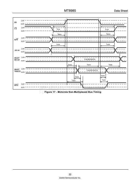
Microprocessor Port
The MT8985 microprocessor port has pin compatibility with Zarlink MT8980 Digital Switch device providing a non-
multiplexed bus architecture. The parallel port consists of an 8 bit parallel data bus (D0-D7), six address input lines
(A0-A5) and four control lines (CS, DS, R/W and DTA). This parallel microport allows the access to the Control
registers, Connection Memory High, Connection Memory Low and the Data Memory. All locations are read/written
except for the data memory which can be read only.
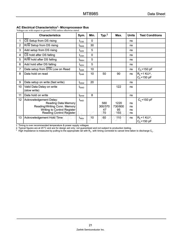
Accesses from the microport to the connection memory and the data memory are multiplexed with accesses from
the input and output TDM ports. This can cause variable Data Acknowledge delays (DTA). In the MT8985 device,
the DTA output provides a maximum acknowledgement delay of 800 ns for read/write operations in the Connection
Memory. However, for operations in the Data Memory (Message Mode), the maximum acknowledgement delay can
be 1220 ns.
6
Zarlink Semiconductor Inc.


 1
1
 2
2
 3
3
 4
4
 5
5
 6
6
 7
7
 8
8
 9
9
 10
10
 11
11
 12
12
 13
13
 14
14
 15
15
 16
16
 17
17
 18
18
 19
19
 20
20
 21
21
 22
22
 23
23
 24
24
 25
25
 26
26
