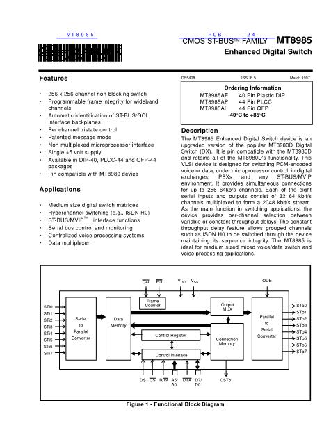
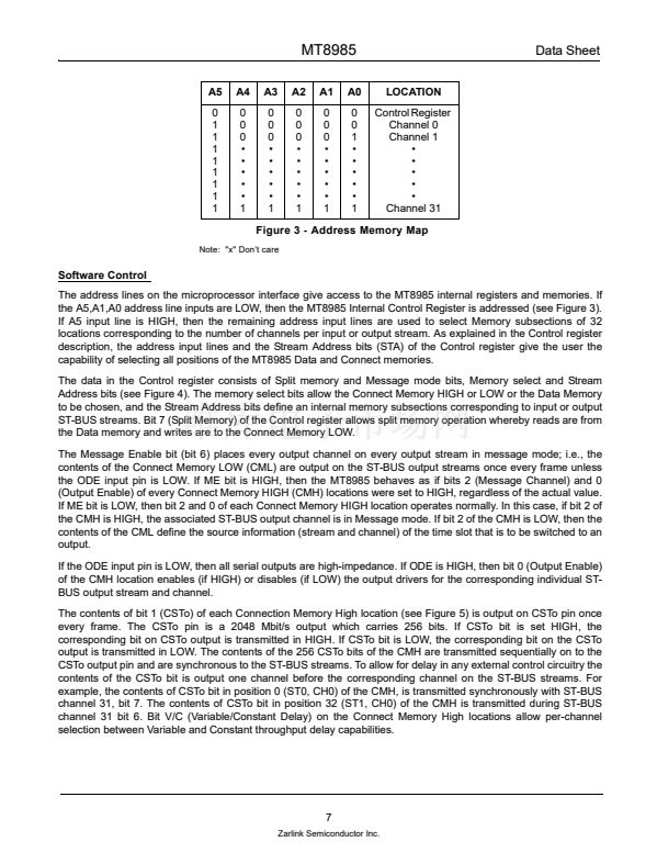
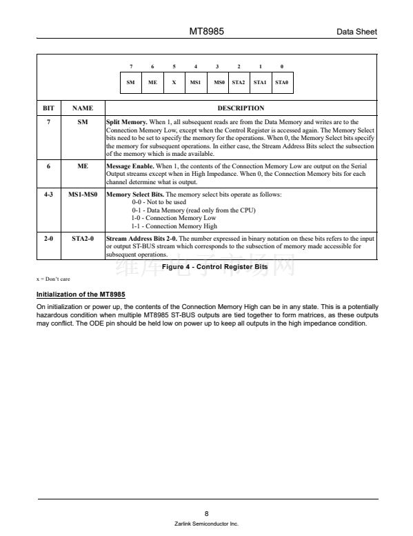
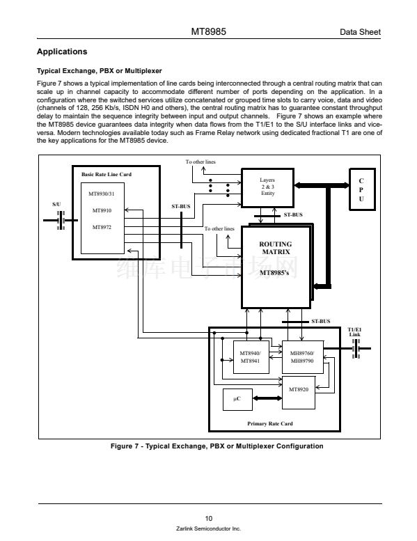
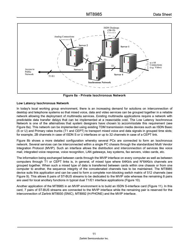
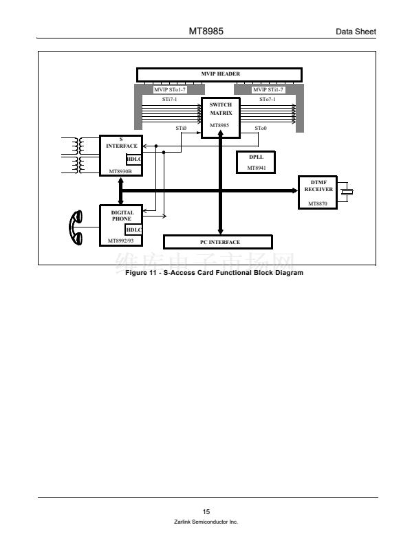
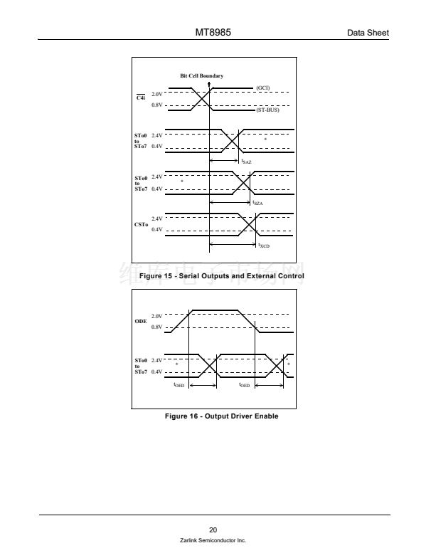
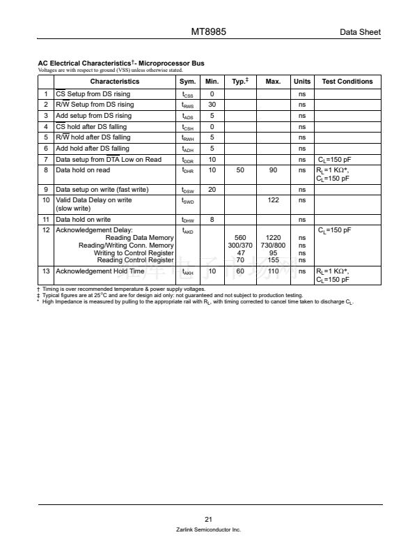
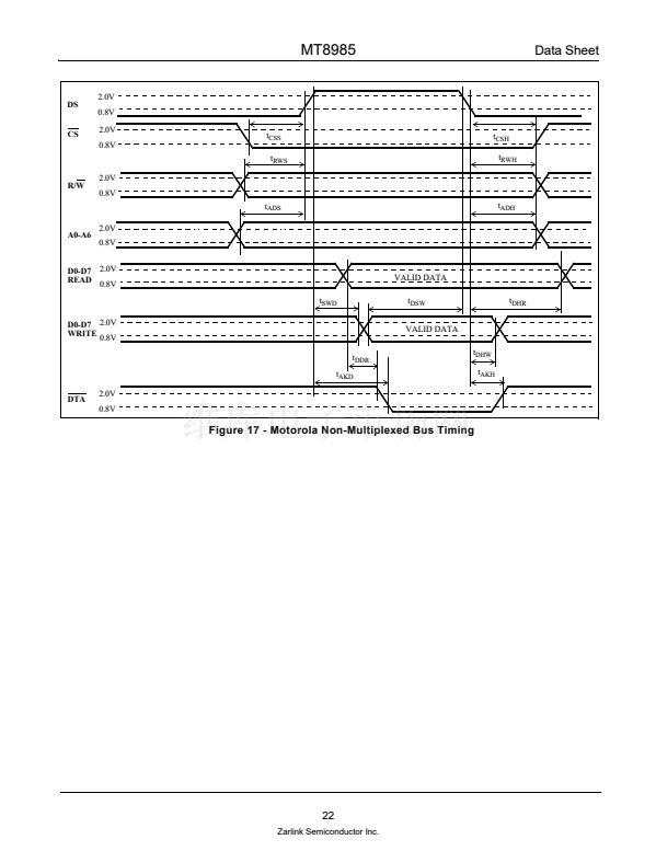
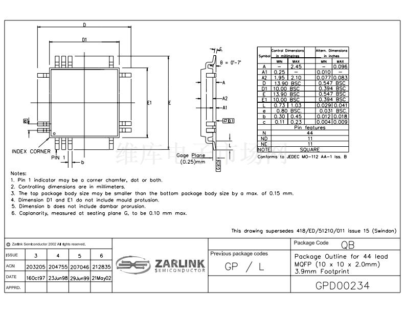
MT8985
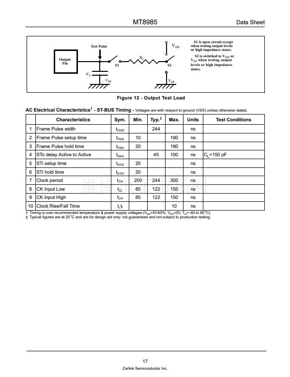
S1 is open circuit except
when testing output levels
or high impedance states.
S2 is switched to V
DD
or
V
SS
when testing output
levels or high impedance
states.
Data Sheet
Test Point
R
L
S1
C
L
V
SS
S2
V
DD
Output
Pin
V
SS
Figure 12 - Output Test Load
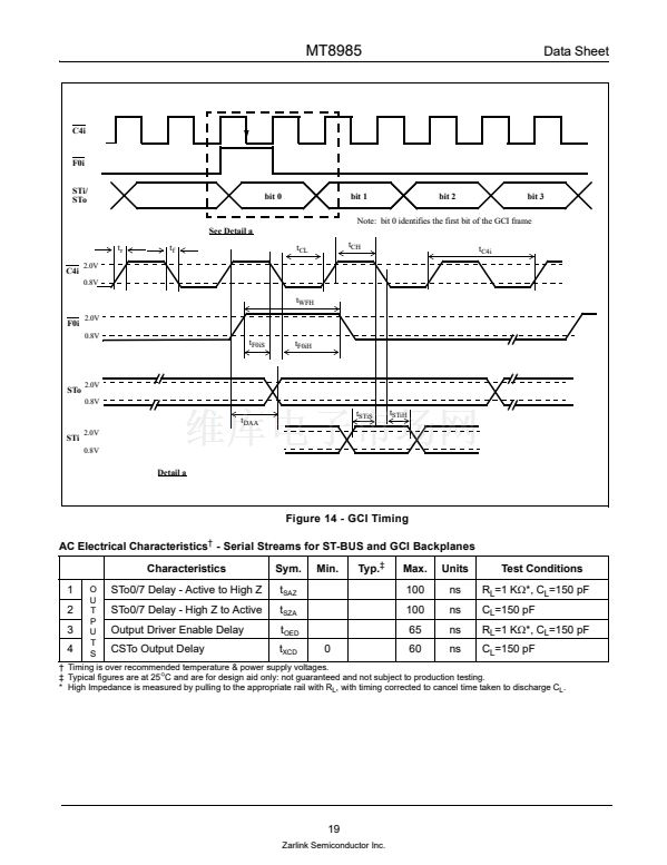
AC Electrical Characteristics
鈥?/div>
- ST-BUS Timing -
Voltages are with respect to ground (VSS) unless otherwise stated.
Characteristics
1 Frame Pulse width
2 Frame Pulse setup time
3 Frame Pulse hold time
4 STo delay Active to Active
5 STi setup time
6 STi hold time
7 Clock period
8 CK Input Low
9 CK Input High
10 Clock Rise/Fall Time
Sym.
t
F0iW
t
F0iS
t
F0iH
t
DAA
t
STiS
t
STiH
t
C4i
t
CL
t
CH
t
r,
t
f
20
20
200
85
85
244
122
122
300
150
150
10
10
20
45
Min.
Typ.
鈥?/div>
244
190
190
100
Max.
Units
ns
ns
ns
ns
ns
ns
ns
ns
ns
ns
C
L
=150 pF
Test Conditions
鈥?Timing is over recommended temperature & power supply voltages (V
DD
=5V
鹵
5%, V
SS
=0V, T
A
=鈥?0 to 85
擄
C).
鈥?Typical figures are at 25
擄
C and are for design aid only: not guaranteed and not subject to production testing.
17
Zarlink Semiconductor Inc.


 1
1
 2
2
 3
3
 4
4
 5
5
 6
6
 7
7
 8
8
 9
9
 10
10
 11
11
 12
12
 13
13
 14
14
 15
15
 16
16
 17
17
 18
18
 19
19
 20
20
 21
21
 22
22
 23
23
 24
24
 25
25
 26
26
