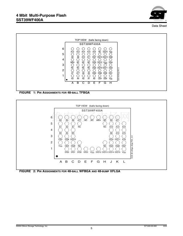
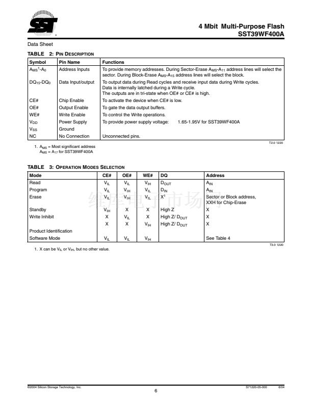
4 Mbit Multi-Purpose Flash
SST39WF400A
Data Sheet
TABLE 6: S
YSTEM
I
NTERFACE
I
NFORMATION FOR
SST39WF400A
Address
1BH
1CH
1DH
1EH
1FH
20H
21H
22H
23H
24H
25H
26H
Data
0016H
0020H
0000H
0000H
0005H
0000H
0005H
0007H
0001H
0000H
0001H
0001H
Data
V
DD
Min (Program/Erase)
DQ
7
-DQ
4
: Volts, DQ
3
-DQ
0
: 100 millivolts
V
DD
Max (Program/Erase)
DQ
7
-DQ
4
: Volts, DQ
3
-DQ
0
: 100 millivolts
V
PP
min (00H = no V
PP
pin)
V
PP
max (00H = no V
PP
pin)
Typical time out for Word-Program 2
N
碌s (2
5
= 32 碌s)
Typical time out for min size buffer program 2
N
碌s (00H = not supported)
Typical time out for individual Sector/Block-Erase 2
N
ms (2
5
= 32 ms)
Typical time out for Chip-Erase 2
N
ms (2
7
= 128 ms)
Maximum time out for Word-Program 2
N
times typical (2
1
x 2
5
= 64 碌s)
Maximum time out for buffer program 2
N
times typical
Maximum time out for individual Sector/Block-Erase 2
N
times typical (2
1
x 2
5
= 64 ms)
Maximum time out for Chip-Erase 2
N
times typical (2
1
x 2
7
= 256 ms)
T6.0 1220
TABLE 7: D
EVICE
G
EOMETRY
I
NFORMATION FOR
SST39WF400A
Address
27H
28H
29H
2AH
2BH
2CH
2DH
2EH
2FH
30H
31H
32H
33H
34H
Data
0013H
0001H
0000H
0000H
0000H
0002H
007FH
0000H
0010H
0000H
0007H
0000H
0000H
0001H
Data
Device size = 2
N
Byte (13H = 19; 2
19
= 512 KByte)
Flash Device Interface description; 0001H = x16-only asynchronous interface
Maximum number of byte in multi-byte write = 2
N
(00H = not supported)
Number of Erase Sector/Block sizes supported by device
Sector Information (y + 1 = Number of sectors; z x 256B = sector size)
y = 127 + 1 = 128 sectors (007FH = 127)
z = 16 x 256 Bytes = 4 KByte/sector (0010H = 16)
Block Information (y + 1 = Number of blocks; z x 256B = block size)
y = 7 + 1 = 8 blocks (0007H = 7)
z = 256 x 256 Bytes = 64 KByte/block (0100H = 256)
T7.0 1220
漏2004 Silicon Storage Technology, Inc.
S71220-05-000
6/04
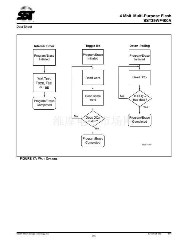
8


 1
1
 2
2
 3
3
 4
4
 5
5
 6
6
 7
7
 8
8
 9
9
 10
10
 11
11
 12
12
 13
13
 14
14
 15
15
 16
16
 17
17
 18
18
 19
19
 20
20
 21
21
 22
22
 23
23
 24
24
 25
25
 26
26
