4 Mbit Multi-Purpose Flash
SST39WF400A
Data Sheet
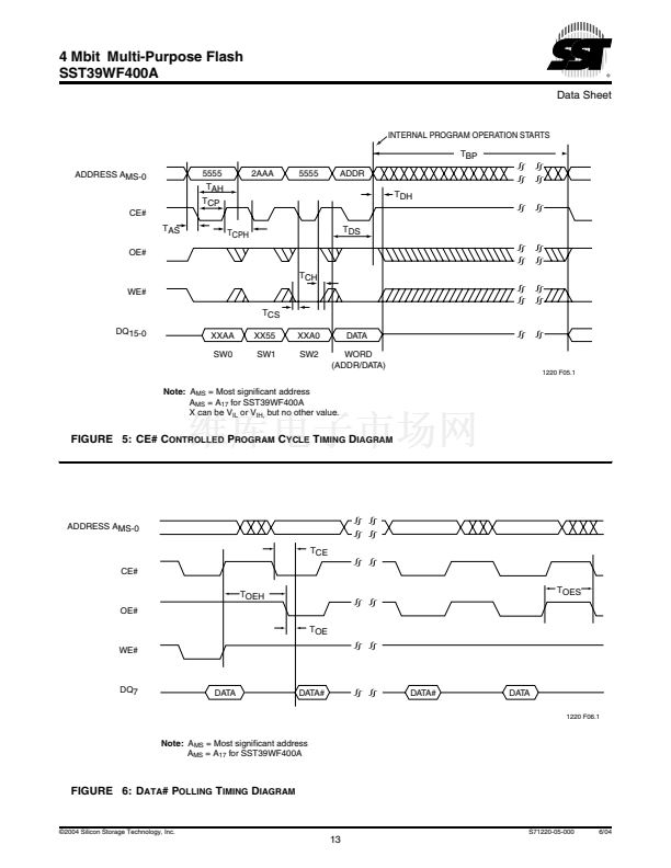
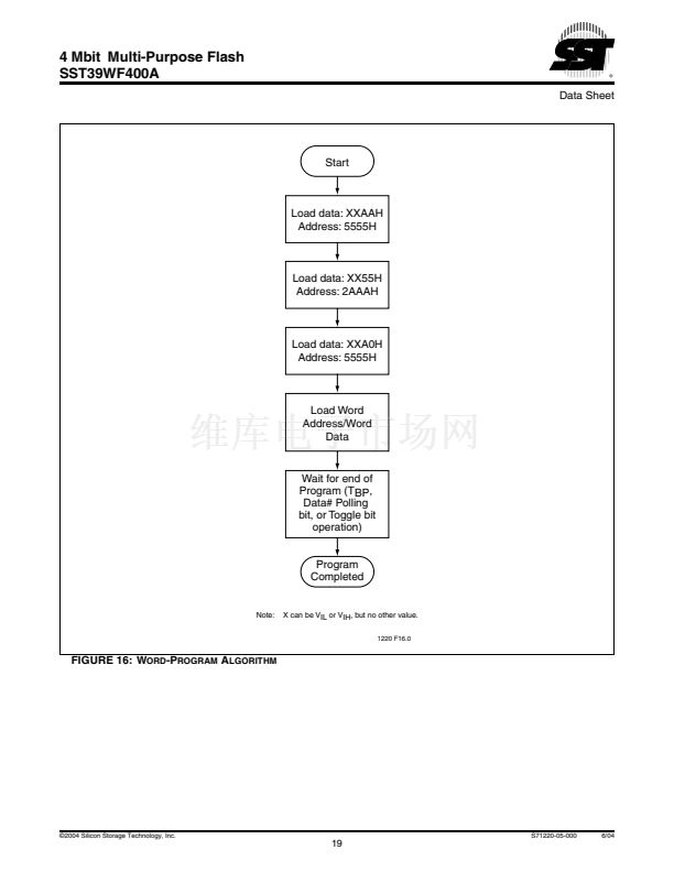
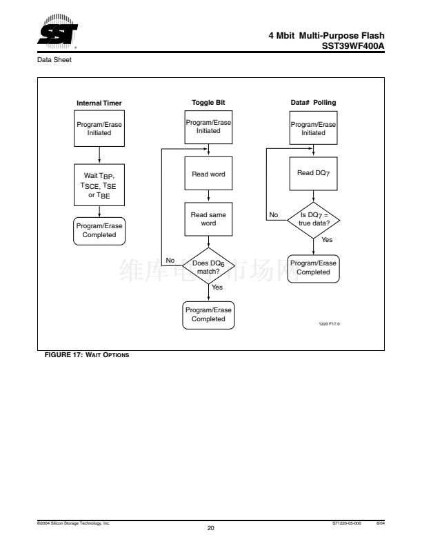
Data# Polling (DQ
7
)
When the SST39WF400A is in the internal Program oper-
ation, any attempt to read DQ
7
will produce the comple-
ment of the true data. Once the Program operation is
completed, DQ
7
will produce true data. Note that even
though DQ
7
may have valid data immediately following the
completion of an internal Write operation, the remaining
data outputs may still be invalid: valid data on the entire
data bus will appear in subsequent successive Read
cycles after an interval of 1 碌s. During internal Erase oper-
ation, any attempt to read DQ
7
will produce a 鈥?鈥? Once the
internal Erase operation is completed, DQ
7
will produce a
鈥?鈥? The Data# Polling is valid after the rising edge of fourth
WE# (or CE#) pulse for Program operation. For Sector-,
Block- or Chip-Erase, the Data# Polling is valid after the
rising edge of sixth WE# (or CE#) pulse. See Figure 6 for
Data# Polling timing diagram and Figure 17 for a flowchart.
Software Data Protection (SDP)
The SST39WF400A provides the JEDEC approved Soft-
ware Data Protection scheme for all data alteration opera-
tions, i.e., Program and Erase. Any Program operation
requires the inclusion of the three-byte sequence. The
three-byte load sequence is used to initiate the Program
operation, providing optimal protection from inadvertent
Write operations, e.g., during the system power-up or
power-down. Any Erase operation requires the inclusion of
six-byte sequence. This group of devices are shipped with
the Software Data Protection permanently enabled. See
Table 4 for the specific software command codes. During
SDP command sequence, invalid commands will abort the
device to Read mode within T
RC
. The contents of DQ
15
-
DQ
8
can be V
IL
or V
IH
, but no other value, during any SDP
command sequence.
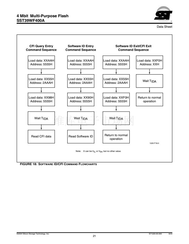
Common Flash Memory Interface (CFI)
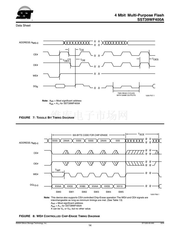
Toggle Bit (DQ
6
)
During the internal Program or Erase operation, any con-
secutive attempts to read DQ
6
will produce alternating 1s
and 0s, i.e., toggling between 1 and 0. When the internal
Program or Erase operation is completed, the DQ
6
bit will
stop toggling. The device is then ready for the next opera-
tion. The Toggle Bit is valid after the rising edge of fourth
WE# (or CE#) pulse for Program operation. For Sector-,
Block- or Chip-Erase, the Toggle Bit is valid after the rising
edge of sixth WE# (or CE#) pulse. See Figure 7 for Toggle
Bit timing diagram and Figure 17 for a flowchart.
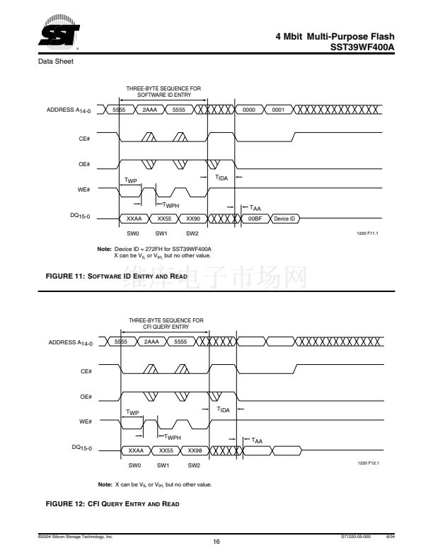
The SST39WF400A also contains the CFI information to
describe the characteristics of the device. In order to enter
the CFI Query mode, the system must write three-byte
sequence, same as Software ID Entry command with 98H
(CFI Query command) to address 5555H in the last byte
sequence. Once the device enters the CFI Query mode,
the system can read CFI data at the addresses given in
Tables 5 through 7. The system must write the CFI Exit
command to return to Read mode from the CFI Query
mode.
Data Protection
The SST39WF400A provides both hardware and software
features to protect nonvolatile data from inadvertent writes.
Hardware Data Protection
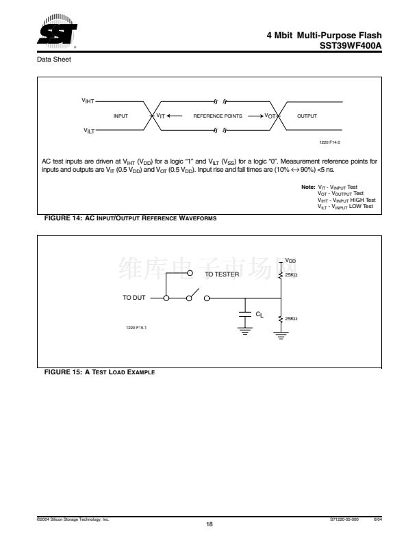
Noise/Glitch Protection: A WE# or CE# pulse of less than 5
ns will not initiate a write cycle.
V
DD
Power Up/Down Detection: The Write operation is
inhibited when V
DD
is less than 1.0V.
Write Inhibit Mode: Forcing OE# low, CE# high, or WE#
high will inhibit the Write operation. This prevents inadvert-
ent writes during power-up or power-down.
漏2004 Silicon Storage Technology, Inc.
S71220-05-000
6/04
3


 1
1
 2
2
 3
3
 4
4
 5
5
 6
6
 7
7
 8
8
 9
9
 10
10
 11
11
 12
12
 13
13
 14
14
 15
15
 16
16
 17
17
 18
18
 19
19
 20
20
 21
21
 22
22
 23
23
 24
24
 25
25
 26
26
