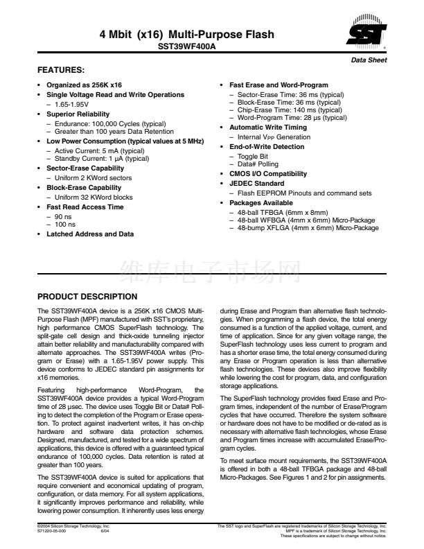
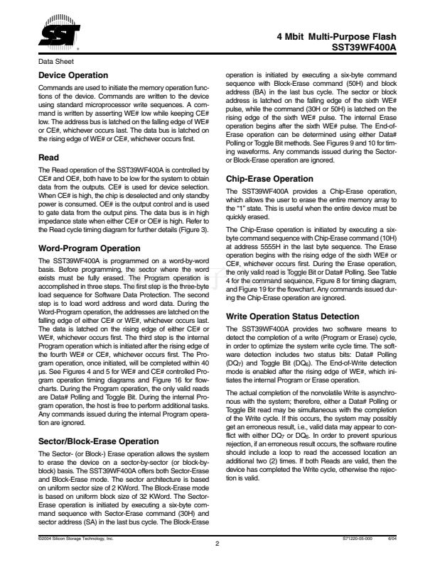
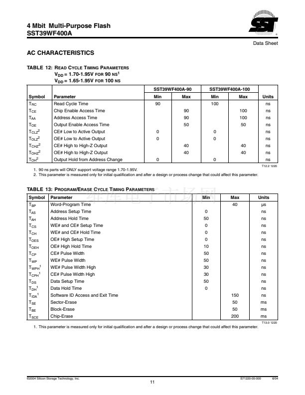
4 Mbit Multi-Purpose Flash
SST39WF400A
Data Sheet
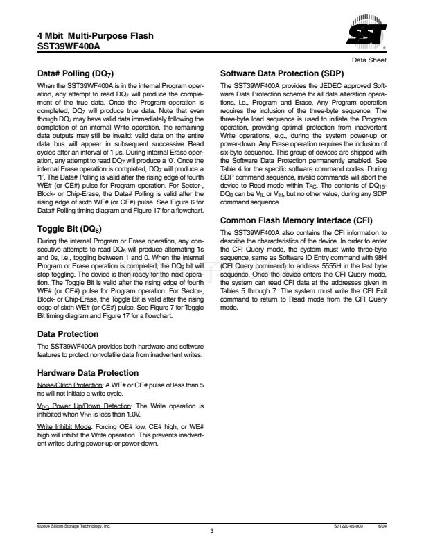
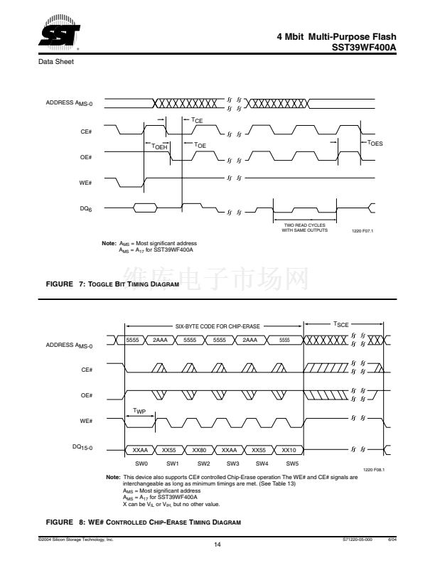
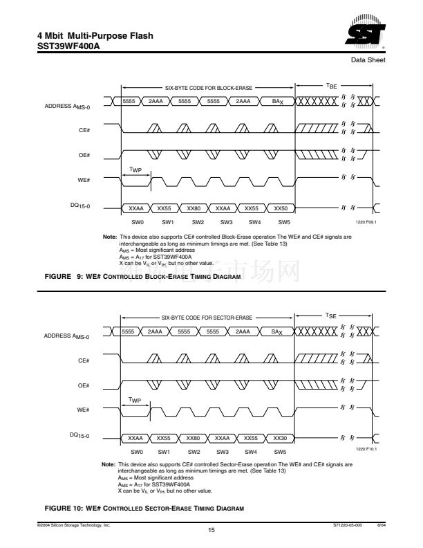
SIX-BYTE CODE FOR BLOCK-ERASE
ADDRESS AMS-0
5555
2AAA
5555
5555
2AAA
BAX
TBE
CE#
OE#
TWP
WE#
DQ15-0
XXAA
SW0
XX55
SW1
XX80
SW2
XXAA
SW3
XX55
SW4
XX50
SW5
1220 F09.1
Note:
This device also supports CE# controlled Block-Erase operation The WE# and CE# signals are
interchangeable as long as minimum timings are met. (See Table 13)
A
MS
= Most significant address
A
MS
= A
17
for SST39WF400A
X can be V
IL
or V
IH,
but no other value.
FIGURE 9: WE# C
ONTROLLED
B
LOCK
-E
RASE
T
IMING
D
IAGRAM
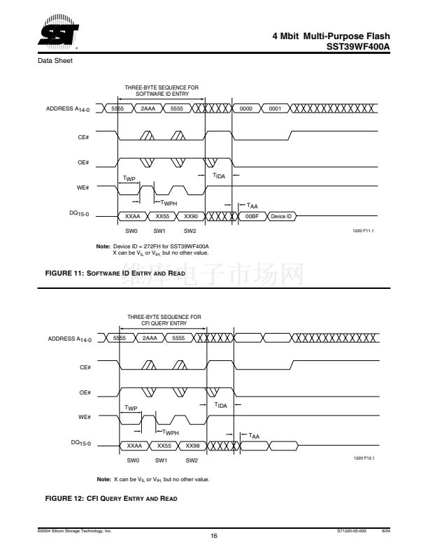
SIX-BYTE CODE FOR SECTOR-ERASE
ADDRESS AMS-0
5555
2AAA
5555
5555
2AAA
SAX
TSE
CE#
OE#
TWP
WE#
DQ15-0
XXAA
SW0
XX55
SW1
XX80
SW2
XXAA
SW3
XX55
SW4
XX30
SW5
1220 F10.1
Note:
This device also supports CE# controlled Sector-Erase operation The WE# and CE# signals are
interchangeable as long as minimum timings are met. (See Table 13)
A
MS
= Most significant address
A
MS
= A
17
for SST39WF400A
X can be V
IL
or V
IH,
but no other value.
FIGURE 10: WE# C
ONTROLLED
S
ECTOR
-E
RASE
T
IMING
D
IAGRAM
漏2004 Silicon Storage Technology, Inc.
S71220-05-000
6/04
15


 1
1
 2
2
 3
3
 4
4
 5
5
 6
6
 7
7
 8
8
 9
9
 10
10
 11
11
 12
12
 13
13
 14
14
 15
15
 16
16
 17
17
 18
18
 19
19
 20
20
 21
21
 22
22
 23
23
 24
24
 25
25
 26
26
