Philips Semiconductors
Product specification
Octal UART for 3.3V and 5V supply voltage
SC28L198
脕
脕
脕脕脕脕脕脕脕脕脕脕脕脕脕脕脕脕脕脕脕脕脕脕脕脕脕脕脕脕脕脕脕脕脕脕
脕
脕
脕 脕脕脕脕脕脕脕脕脕脕脕脕脕脕脕脕脕脕脕脕脕脕脕脕脕脕
脕脕脕脕脕脕脕脕
脕脕脕脕脕脕脕脕脕脕脕脕脕脕脕脕脕脕脕脕脕脕脕脕脕脕脕脕脕脕脕脕脕脕
脕
脕脕脕脕脕脕脕脕脕脕脕脕脕脕脕脕脕脕脕脕脕脕脕脕脕脕脕脕脕脕脕脕脕脕
脕脕脕脕脕脕脕脕脕脕脕脕脕脕脕脕脕脕脕脕脕脕脕脕脕脕脕
脕
脕脕脕脕脕脕脕脕脕脕脕脕脕脕脕脕脕脕脕脕脕脕脕脕脕脕脕脕脕脕脕脕脕脕
脕
脕脕脕脕脕脕脕脕脕脕脕脕脕脕脕脕脕脕脕脕脕脕脕脕脕脕脕脕脕脕脕脕脕脕
脕
脕脕脕脕脕脕脕脕脕脕脕脕脕脕脕脕脕脕脕脕脕脕脕脕脕脕脕脕脕脕脕脕脕脕
脕
脕脕脕脕脕脕脕脕脕脕脕脕脕脕脕脕脕脕脕脕脕脕脕脕脕脕脕脕脕脕脕脕脕脕
脕
脕脕脕脕脕脕脕脕脕脕脕脕脕脕脕脕脕脕脕脕脕脕脕脕脕脕脕脕脕脕脕脕脕脕
脕
脕脕脕脕脕脕脕脕脕脕脕脕脕脕脕脕脕脕脕脕脕脕脕脕脕脕脕脕脕脕脕脕脕脕
脕
脕脕脕脕脕脕脕脕脕脕脕脕脕脕脕脕脕脕脕脕脕脕脕脕脕脕脕脕脕脕脕脕脕脕
脕
脕脕脕脕脕脕脕脕脕脕脕脕脕脕脕脕脕脕脕脕脕脕脕脕脕脕脕脕脕脕脕脕脕脕
脕
脕脕脕脕脕脕脕脕脕脕脕脕脕脕脕脕脕脕脕脕脕脕脕脕脕脕脕脕脕脕脕脕脕脕
脕
脕脕脕脕脕脕脕脕脕脕脕脕脕脕脕脕脕脕脕脕脕脕脕脕脕脕脕脕脕脕脕脕脕脕
脕
脕脕脕脕脕脕脕脕脕脕脕脕脕脕脕脕脕脕脕脕脕脕脕脕脕脕脕脕脕脕脕脕脕脕
脕
脕
脕脕脕脕脕脕脕脕脕脕脕脕脕脕脕脕脕脕脕脕脕脕脕脕脕脕脕脕脕脕脕脕脕脕
脕
脕
脕脕脕脕脕脕脕脕脕脕脕脕脕脕脕脕脕脕脕脕脕脕脕脕脕脕脕脕脕脕脕脕脕脕
脕脕脕脕脕脕脕脕
脕脕脕脕脕脕脕脕脕脕脕脕脕脕脕脕脕脕脕脕脕脕脕脕脕脕脕脕脕脕脕脕脕脕
脕
脕脕脕脕脕脕脕脕脕脕脕脕脕脕脕脕脕脕脕脕脕脕脕脕脕脕脕脕脕脕脕脕脕脕
脕
脕脕脕脕脕脕脕脕脕脕脕脕脕脕脕脕脕脕脕脕脕脕脕脕脕脕脕脕脕脕脕脕脕脕
脕
脕脕脕脕脕脕脕脕脕脕脕脕脕脕脕脕脕脕脕脕脕脕脕脕脕脕脕脕脕脕脕脕脕脕
脕
脕脕脕脕脕脕脕脕脕脕脕脕脕脕脕脕脕脕脕脕脕脕脕脕脕脕脕脕脕脕脕脕脕脕
脕
脕脕脕脕脕脕脕脕脕脕脕脕脕脕脕脕脕脕脕脕脕脕脕脕脕脕脕脕脕脕脕脕脕脕
脕脕脕脕脕脕脕脕脕脕脕脕脕脕脕脕脕脕脕脕脕脕脕脕脕脕
脕
脕
脕脕脕脕脕脕脕脕脕脕脕脕脕脕脕脕脕脕脕脕脕脕脕脕脕脕脕脕脕脕脕脕脕脕
脕脕脕脕脕脕脕脕
脕脕脕脕脕脕脕脕脕脕脕脕脕脕脕脕脕脕脕脕脕脕脕脕脕脕脕脕脕脕脕脕脕脕
脕
脕脕脕脕脕脕脕脕脕脕脕脕脕脕脕脕脕脕脕脕脕脕脕脕脕脕脕脕脕脕脕脕脕脕
脕
脕
脕脕脕脕脕脕脕脕脕脕脕脕脕脕脕脕脕脕脕脕脕脕脕脕脕脕脕脕脕脕脕脕脕脕
脕脕脕脕脕脕脕脕脕脕脕脕脕脕脕脕脕脕脕脕脕脕脕脕脕脕
脕
脕
脕脕脕脕脕脕脕脕脕脕脕脕脕脕脕脕脕脕脕脕脕脕脕脕脕脕脕脕脕脕脕脕脕脕
脕脕脕脕脕脕脕脕
脕脕脕脕脕脕脕脕脕脕脕脕脕脕脕脕脕脕脕脕脕脕脕脕脕脕脕脕脕脕脕脕脕脕
脕
脕脕脕脕脕脕脕脕脕脕脕脕脕脕脕脕脕脕脕脕脕脕脕脕脕脕脕脕脕脕脕脕脕脕
脕
脕
脕脕脕脕脕脕脕脕脕脕脕脕脕脕脕脕脕脕脕脕脕脕脕脕脕脕脕脕脕脕脕脕脕脕
脕
脕脕脕脕脕脕脕脕脕脕脕脕脕脕脕脕脕脕脕脕脕脕脕脕脕脕脕脕脕脕脕脕脕脕
脕
脕脕脕脕脕脕脕脕脕脕脕脕脕脕脕脕脕脕脕脕脕脕脕脕脕脕脕脕脕脕脕脕脕脕
脕
脕脕脕脕脕脕脕脕脕脕脕脕脕脕脕脕脕脕脕脕脕脕脕脕脕脕脕脕脕脕脕脕脕脕
脕
脕脕脕脕脕脕脕脕脕脕脕脕脕脕脕脕脕脕脕脕脕脕脕脕脕脕脕脕脕脕脕脕脕脕
脕脕脕脕脕脕脕脕脕脕脕脕脕脕脕脕脕脕脕脕脕脕脕脕脕脕脕脕
脕
脕
脕脕脕脕脕脕脕脕脕脕脕脕脕脕脕脕脕脕脕脕脕脕脕脕脕脕脕脕脕脕脕脕脕脕
脕脕脕脕脕脕脕脕脕脕脕脕脕脕脕脕脕脕脕脕脕脕脕脕脕脕脕脕脕脕脕脕脕脕
脕脕脕脕脕脕脕脕脕脕脕脕脕脕脕脕脕脕脕脕脕脕脕脕脕脕 脕脕脕脕脕
脕
脕脕脕脕脕脕脕脕脕脕脕脕脕脕脕脕脕脕脕脕脕脕脕脕脕脕脕脕脕脕脕脕脕脕
脕
脕脕脕脕脕脕脕脕脕脕脕脕脕脕脕脕脕脕脕脕脕脕脕脕脕脕脕脕脕脕脕脕脕脕
脕
脕脕脕脕脕脕脕脕脕脕脕脕脕脕脕脕脕脕脕脕脕脕脕脕脕脕脕脕脕脕脕脕脕脕
脕脕脕脕脕脕脕脕
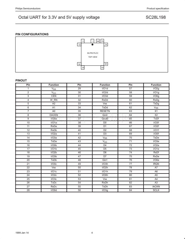
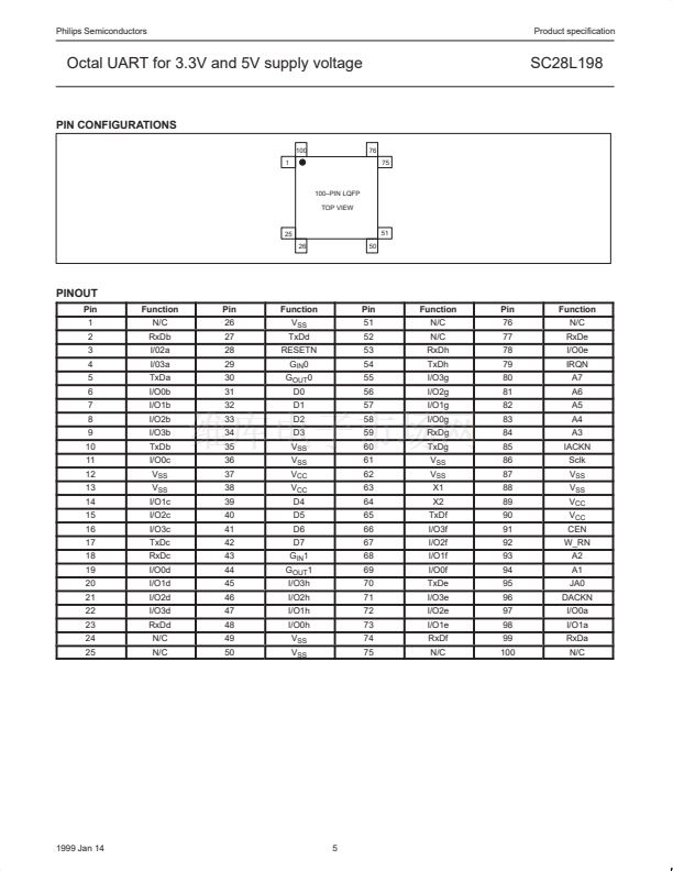
MNEMONIC
SClk
TYPE
I
I
I
DESCRIPTION
Host system clock. Used to time operations in the Host Interface and clock internal logic. Must be greater
than twice the frequency of highest X1, Counter/Timer, TxC (1x) or RxC (1x) input frequency.
CEN
Chip select: Active low. When asserted, allows I/O access to OCTART registers by host CPU. W_RN signal
indicates direction. (Must
not be active in IACKN cycle)
Address lines (A[6] is
NOT
used. See 鈥滺ost Interface鈥?)
8鈥揵it bi鈥揹irectional data bus. Carries command and status information between 28L198 and the host CPU.
Used to convey parallel data for serial I/O between the host CPU and the 28L198
A(7:0)
D(7:0)
I/O
I
W_RN
Write Read not control: When high indicates that the host CPU will write to a 28L198 register or transmit FIFO.
When low, indicates a read cycle. 0 = Read; 1 = Write
Data Acknowledge: Active low. When asserted, it signals that the last transfer of the D lines is complete.
Open drain.
DACKN
IRQN
O
O
I
Interrupt Request: Active low. When asserted, indicates that the 28L198 requires service for pending inter-
rupt(s). Open drain.
IACKN
Interrupt Acknowledge: Active low. When asserted, indicates that the host CPU has initiated an interrupt ac-
knowledge cycle.
(Do not use CEN in an IACKN cycle)
Transmit Data: Serial outputs from the 8 UARTs.
Receive Data: Serial inputs to the 8 UARTs
TD(a鈥揾)
O
I
RD(a鈥揾)
I/O0(a鈥揾)
I/O1(a鈥揾)
I/O2(a鈥揾)
I/O3(a鈥揾)
G
IN
(1:0)
G
OUT
0
I/O
I/O
I/O
I/O
I
I
I
O
Input/Output 0: Multi鈥搖se input or output pin for the UART.
Input/Output 1: Multi鈥搖se input or output pin for the UART.
Input/Output 2: Multi鈥搖se input or output pin for the UART.
Input/Output 3: Multi鈥搖se input or output pin for the UART.
Global general purpose inputs, available to any/all channels.
Global general purpose outputs, available from any channel.
RESETN
Master reset: Active Low. Must be asserted at power up and may be asserted at other times to reset and re-
start the system. See 鈥淩eset Conditions鈥?at end of register map. Minimum width 10 SCLK.
X1/CCLK
X2
Crystal 1 or Communication Clock: This pin may be connected to one side of a 2鈥? MHz crystal. It may alter-
natively be driven by an external clock in this frequency range. Standard frequency = 3.6864 MHz
O
I
Crystal 2: If a crystal is used, this is the connection to the second terminal. If a clock signal drives X1, this pin
must be left unconnected.
8 pins total 6 pins for Vss, 2 pins for Vcc
Power Supplies
NOTE: Many output pins will have very fast edges, especially when lightly loaded (less than 20 pf.) These edges may move as fast as 1 to 3 ns
fall or rise time. The user must be aware of the possible generation of ringing and reflections on improperly terminated interconnections. See
previous note on Sclk noise under pin assignments.
Pin Description
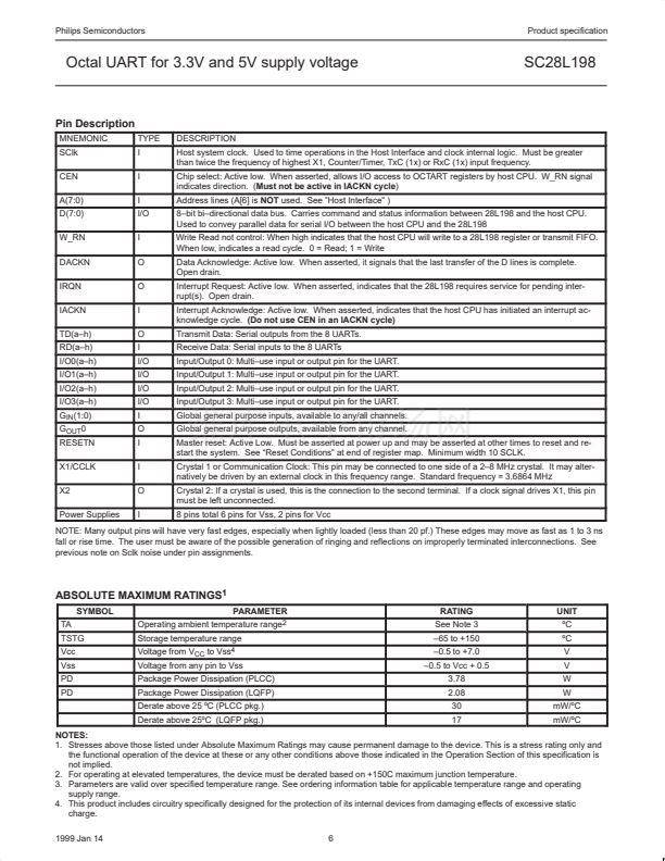
ABSOLUTE MAXIMUM RATINGS
1
脕脕脕脕脕脕
脕
脕
脕
脕脕脕脕脕脕脕脕脕脕脕脕脕脕脕脕脕脕脕脕脕脕脕脕脕脕脕脕脕脕脕脕脕脕
脕
脕
脕
脕脕脕脕脕脕
脕
脕
脕
脕脕脕脕脕脕脕脕脕脕脕脕脕脕脕脕脕脕脕脕脕脕脕脕脕脕脕脕脕脕脕脕脕脕
脕
脕
脕
脕脕脕脕脕脕
脕脕脕脕脕脕脕脕脕脕脕脕脕脕脕脕脕脕脕脕脕脕脕脕脕脕脕脕脕脕脕脕脕脕
脕
脕
脕
脕
脕
脕
脕脕脕脕脕脕脕脕脕脕脕脕脕脕脕脕脕脕脕脕脕脕脕脕脕脕脕脕脕脕脕脕脕脕
脕脕脕脕脕脕脕脕脕脕脕脕脕脕脕脕脕脕脕脕脕脕脕脕脕脕脕脕脕
脕
脕
脕脕脕脕脕脕脕脕脕脕脕脕脕脕脕脕脕脕脕脕脕脕脕脕脕脕脕脕脕脕脕脕脕脕
脕
脕
脕
脕脕脕脕脕脕脕脕脕脕脕脕脕脕脕脕脕脕脕脕脕脕脕脕脕脕脕脕脕脕脕脕脕脕
脕
脕
脕
脕脕脕脕脕脕脕脕脕脕脕脕脕脕脕脕脕脕脕脕脕脕脕脕脕脕脕脕脕脕脕脕脕脕
脕
脕
脕
脕脕脕脕脕脕脕脕脕脕脕脕脕脕脕脕脕脕脕脕脕脕脕脕脕脕脕脕脕脕脕脕脕脕
脕
脕
脕
脕脕脕脕脕脕脕脕脕脕脕脕脕脕脕脕脕脕脕脕脕脕脕脕脕脕脕脕脕脕脕脕脕脕
脕
脕
脕
脕脕脕脕脕脕脕脕脕脕脕脕脕脕脕脕脕脕脕脕脕脕脕脕脕脕脕脕脕脕脕脕脕脕
脕脕脕脕脕脕脕脕脕脕脕脕脕脕脕脕脕脕脕脕脕脕脕脕脕脕脕脕脕
脕
脕
脕脕脕脕脕脕脕脕脕脕脕脕脕脕脕脕脕脕脕脕脕脕脕脕脕脕脕脕脕脕脕脕脕脕
脕
脕
脕
脕脕脕脕脕脕脕脕脕脕脕脕脕脕脕脕脕脕脕脕脕脕脕脕脕脕脕脕脕脕脕脕脕脕
脕脕脕脕脕脕脕脕脕脕脕脕脕脕脕脕脕脕脕脕脕脕脕脕脕脕脕脕脕脕脕脕脕脕
脕
脕脕脕脕脕脕脕脕脕脕脕脕脕脕脕脕脕脕脕脕脕脕脕脕脕脕脕脕脕
脕
脕
脕
脕
SYMBOL
PARAMETER
range
2
RATING
UNIT
潞C
潞C
V
V
TA
Operating ambient temperature
Storage temperature range
Voltage from V
CC
to Vss
4
See Note 3
TSTG
Vcc
Vss
PD
PD
鈥?5 to +150
鈥?.5 to +7.0
3.78
2.08
30
17
Voltage from any pin to Vss
鈥?.5 to Vcc + 0.5
Package Power Dissipation (PLCC)
Package Power Dissipation (LQFP)
Derate above 25 潞C (PLCC pkg.)
Derate above 25潞C (LQFP pkg.)
W
W
mW/潞C
mW/潞C
NOTES:
1. Stresses above those listed under Absolute Maximum Ratings may cause permanent damage to the device. This is a stress rating only and
the functional operation of the device at these or any other conditions above those indicated in the Operation Section of this specification is
not implied.
2. For operating at elevated temperatures, the device must be derated based on +150C maximum junction temperature.
3. Parameters are valid over specified temperature range. See ordering information table for applicable temperature range and operating
supply range.
4. This product includes circuitry specifically designed for the protection of its internal devices from damaging effects of excessive static
charge.
1999 Jan 14
6


 1
1
 2
2
 3
3
 4
4
 5
5
 6
6
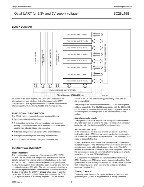 7
7
 8
8
 9
9
 10
10
 11
11
 12
12
 13
13
 14
14
 15
15
 16
16
 17
17
 18
18
 19
19
 20
20
 21
21
 22
22
 23
23
 24
24
 25
25
 26
26
 27
27
 28
28
 29
29
 30
30
 31
31
 32
32
 33
33
 34
34
 35
35
 36
36
 37
37
 38
38
 39
39
 40
40
 41
41
 42
42
 43
43
 44
44
 45
45
 46
46
 47
47
 48
48
 49
49
 50
50
 51
51
 52
52
 53
53
 54
54
 55
55
 56
56
