RxFIFO fill level. This field allows interrupt arbitration to begin when
character.
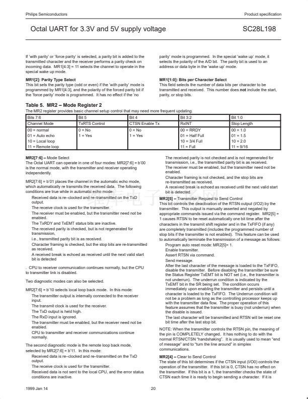
MR2[1:0] 鈥?/div>
Stop Bit Length Select
This field programs the length of the stop bit appended to the
transmitted character. Stop bit lengths of 9/16, 1, 1.5 and 2 bits can
be programmed for character lengths of 6, 7, and 8 bits. For a
character length of 5 bits, 1, 1.5 and 2 stop bits can be programmed.
In all cases, the receiver only checks for a mark condition at the
center of the first stop bit position (one bit time after the last data bit,
or after the parity bit if parity is enabled). If an external 1X clock is
used for the transmitter, MR2[1] = 0 selects one stop bit and MR2[1]
= 1 selects two stop bits to be transmitted.
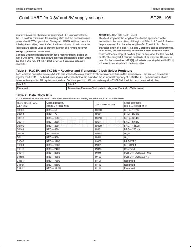
Table 6. RxCSR and TxCSR 鈥?Receiver and Transmitter Clock Select Registers
Both registers consist of single 5 bit field that selects the clock source for the receiver and transmitter, respectively. The unused bits in this
register read b鈥?11. The baud rates shown in the table below are based on the x1 crystal frequency of 3.6864MHz. The baud rates shown
below will vary as the X1 crystal clock varies. For example, if the X1 rate is changed to 7.3728 MHz all the rates below will double.
脕脕脕脕脕脕脕脕脕脕脕脕
脕
脕
脕
脕脕脕脕脕脕脕脕脕脕脕脕脕脕脕脕脕脕脕脕脕脕脕脕脕脕脕脕脕脕脕脕脕脕
脕
脕
脕
脕脕脕脕脕脕脕脕脕脕脕脕
脕
脕
脕
脕脕脕脕脕脕脕脕脕脕脕脕脕脕脕脕脕脕脕脕脕脕脕脕脕脕脕脕脕脕脕脕脕脕
脕
脕
脕
脕脕脕脕脕脕脕脕脕脕脕脕
脕脕脕脕脕脕脕脕脕脕脕脕脕脕脕脕脕脕脕脕脕脕脕脕脕脕脕脕脕脕脕脕脕脕
脕
脕
脕
脕
脕
脕
脕脕脕脕脕脕脕脕脕脕脕脕脕脕脕脕脕脕脕脕脕脕脕脕脕脕脕脕脕脕脕脕脕脕
脕脕脕脕脕脕脕脕脕脕脕脕脕脕脕脕脕脕脕脕脕脕脕
脕
脕
脕脕脕脕脕脕脕脕脕脕脕脕脕脕脕脕脕脕脕脕脕脕脕脕脕脕脕脕脕脕脕脕脕脕
脕
脕
脕
脕脕脕脕脕脕脕脕脕脕脕脕脕脕脕脕脕脕脕脕脕脕脕脕脕脕脕脕脕脕脕脕脕脕
脕
脕
脕
脕脕脕脕脕脕脕脕脕脕脕脕脕脕脕脕脕脕脕脕脕脕脕脕脕脕脕脕脕脕脕脕脕脕
脕
脕
脕
脕脕脕脕脕脕脕脕脕脕脕脕脕脕脕脕脕脕脕脕脕脕脕脕脕脕脕脕脕脕脕脕脕脕
脕
脕
脕
脕脕脕脕脕脕脕脕脕脕脕脕脕脕脕脕脕脕脕脕脕脕脕脕脕脕脕脕脕脕脕脕脕脕
脕
脕
脕
脕脕脕脕脕脕脕脕脕脕脕脕脕脕脕脕脕脕脕脕脕脕脕脕脕脕脕脕脕脕脕脕脕脕
脕
脕
脕
脕脕脕脕脕脕脕脕脕脕脕脕
脕脕脕脕脕脕脕脕脕脕脕脕脕脕脕脕脕脕脕脕脕脕脕脕脕脕脕脕脕脕脕脕脕脕
脕
脕
脕
脕
脕
脕
脕脕脕脕脕脕脕脕脕脕脕脕脕脕脕脕脕脕脕脕脕脕脕脕脕脕脕脕脕脕脕脕脕脕
脕脕脕脕脕脕脕脕脕脕脕脕脕脕脕脕脕脕脕脕脕脕脕
脕
脕
脕脕脕脕脕脕脕脕脕脕脕脕脕脕脕脕脕脕脕脕脕脕脕脕脕脕脕脕脕脕脕脕脕脕
脕
脕
脕
脕脕脕脕脕脕脕脕脕脕脕脕脕脕脕脕脕脕脕脕脕脕脕脕脕脕脕脕脕脕脕脕脕脕
脕
脕
脕
脕脕脕脕脕脕脕脕脕脕脕脕脕脕脕脕脕脕脕脕脕脕脕脕脕脕脕脕脕脕脕脕脕脕
脕
脕
脕
脕脕脕脕脕脕脕脕脕脕脕脕脕脕脕脕脕脕脕脕脕脕脕脕脕脕脕脕脕脕脕脕脕脕
脕脕脕脕脕脕脕脕脕脕脕脕脕脕脕脕脕脕脕脕脕脕脕
脕
脕
脕脕脕脕脕脕脕脕脕脕脕脕脕脕脕脕脕脕脕脕脕脕脕脕脕脕脕脕脕脕脕脕脕脕
脕
脕
脕
脕脕脕脕脕脕脕脕脕脕脕脕脕脕脕脕脕脕脕脕脕脕脕脕脕脕脕脕脕脕脕脕脕脕
脕脕脕脕脕脕脕脕脕脕脕脕脕脕脕脕脕脕脕脕脕脕脕
脕
脕
脕脕脕脕脕脕脕脕脕脕脕脕脕脕脕脕脕脕脕脕脕脕脕脕脕脕脕脕脕脕脕脕脕脕
脕
脕脕脕脕脕脕脕脕脕脕脕脕脕脕脕脕脕脕脕脕脕脕脕脕
脕
脕脕脕脕脕脕脕脕脕脕脕脕脕脕脕脕脕脕脕脕脕脕脕脕脕脕脕脕脕脕脕脕脕脕
脕脕脕脕脕脕脕脕脕脕脕
Bits 7:5
Bits 4:0
Reserved
Transmitter/Receiver Clock select code, (see Clock Mux Table below)
Table 7. Data Clock Mux
Clock Select Code
CSR (4:0)
00000
00001
00010
00011
00100
00101
00110
00111
CCLK maximum rate is 8MHz. Data clock rates will follow exactly the ratio of CCLK to 3.6864MHz.
Clock selection,
CCLK = 3.6864 MHz
BRG 鈥?50
BRG 鈥?75
Clock Select Code
10000
10001
10010
10011
10100
10101
10110
10111
Clock selection,
CCLK = 3.6864 MHz
BRG 鈥?19.2K
BRG 鈥?28.8K
BRG 鈥?38.4K
BRG 鈥?57.6K
BRG 鈥?150
BRG 鈥?200
BRG 鈥?300
BRG 鈥?450
BRG 鈥?600
BRG 鈥?900
BRG 鈥?115.2K
G
IN
0
G
IN
1
BRG 鈥?230.4K
01000
01001
01010
01011
01100
01101
01110
01111
BRG 鈥?1200
BRG 鈥?1800
BRG 鈥?2400
BRG 鈥?3600
BRG 鈥?4800
BRG 鈥?7200
BRG 鈥?9600
11000
11001
11010
11011
11100
11101
11110
11111
BRG C/T 0
BRG C/T 1
Reserved
I/O2 rcvr, I/O3 xmit 鈥?6x
I/O2 rcvr, I/O3 xmit鈥?x
Reserved
Reserved
Reserved
BRG 鈥?14.4K
1999 Jan 14
21


 1
1
 2
2
 3
3
 4
4
 5
5
 6
6
 7
7
 8
8
 9
9
 10
10
 11
11
 12
12
 13
13
 14
14
 15
15
 16
16
 17
17
 18
18
 19
19
 20
20
 21
21
 22
22
 23
23
 24
24
 25
25
 26
26
 27
27
 28
28
 29
29
 30
30
 31
31
 32
32
 33
33
 34
34
 35
35
 36
36
 37
37
 38
38
 39
39
 40
40
 41
41
 42
42
 43
43
 44
44
 45
45
 46
46
 47
47
 48
48
 49
49
 50
50
 51
51
 52
52
 53
53
 54
54
 55
55
 56
56
