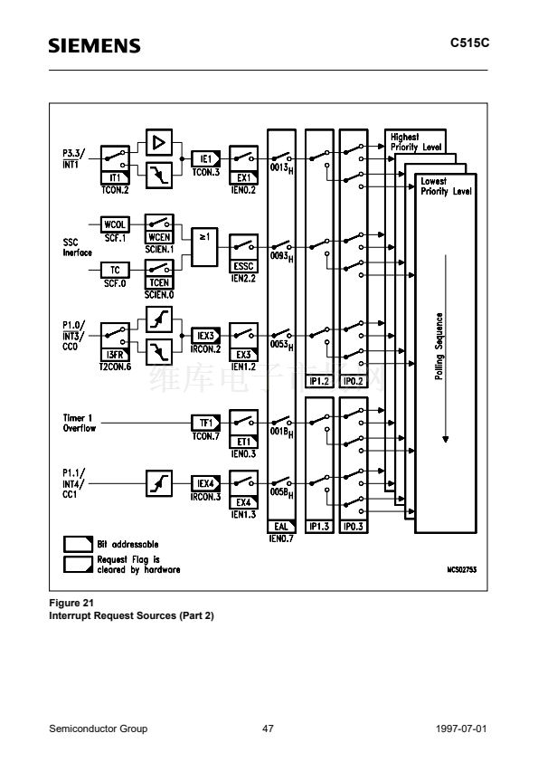
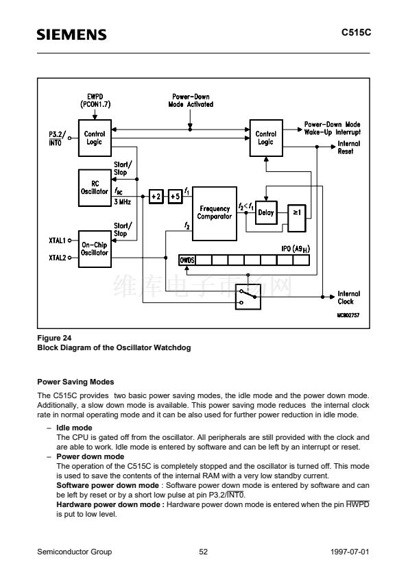
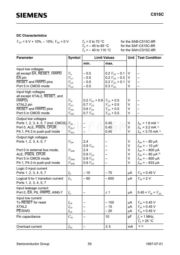
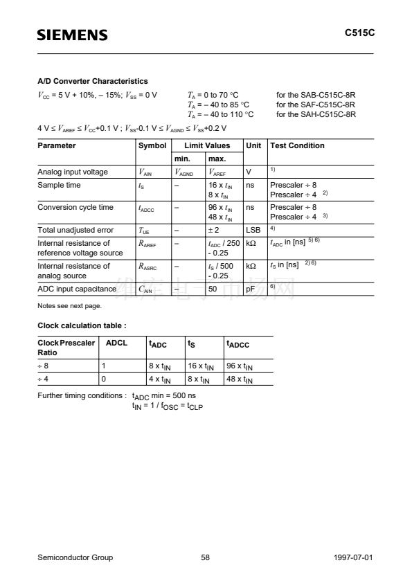
C515C
Power Supply Current
Parameter
Active mode
Idle mode
Active mode with
slow-down enabled
Idle mode with
slow-down enabled
Power-down mode
6 MHz
10 MHz
6 MHz
10 MHz
6 MHz
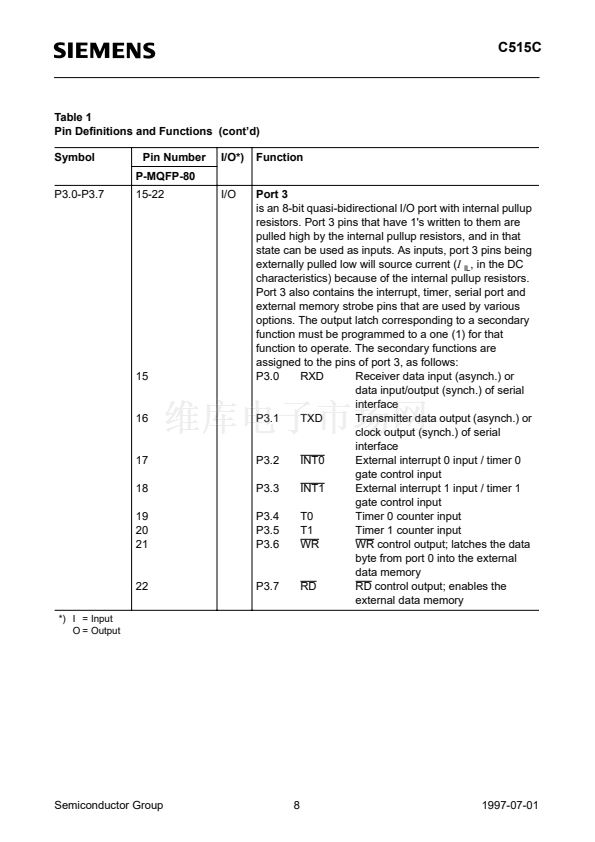
10 MHz
6 MHz
10 MHz
Symbol
Limit Values
typ.
10)
max.
11)
16.1
25.5
9.8
15
TBD
TBD
TBD
TBD
50
mA
mA
mA
mA
mA
mA
mA
mA
碌A
4)
Unit Test Condition
I
CC
I
CC
I
CC
I
CC
I
CC
I
CC
I
CC
I
CC
I
PD
12.0
18.9
6.9
10.5
TBD
TBD
TBD
TBD
TBD
5)
6)
7)
V
CC
= 2鈥?.5 V
3)
1) Capacitive loading on ports 0 and 2 may cause spurious noise pulses to be superimposed on the
V
OL
of ALE
and port 3. The noise is due to external bus capacitance discharging into the port 0 and port 2 pins when these
pins make 1-to-0 transitions during bus operation. In the worst case (capacitive loading > 100 pF), the noise
pulse on ALE line may exceed 0.8 V. In such cases it may be desirable to qualify ALE with a schmitt-trigger,
or use an address latch with a schmitt-trigger strobe input.
2) Capacitive loading on ports 0 and 2 may cause the
V
OH
on ALE and PSEN to momentarily fall below the
0.9
V
CC
specification when the address lines are stabilizing.
3)
I
PD
(power-down mode) is measured under following conditions:
EA = RESET = Port 0 = Port 6 =
V
CC
; XTAL1 = N.C.; XTAL2 =
V
SS
; PE/SWD =
V
SS
; HWPD =
V
CC
;
V
AGND
=
V
SS
;
V
AREF
=
V
CC
; all other pins are disconnected.
I
PD
(hardware power-down mode) is independent of any particular pin connection.
4)
I
CC
(active mode) is measured with:
XTAL2 driven with
t
CLCH
,
t
CHCL
= 5 ns ,
V
IL
=
V
SS
+ 0.5 V,
V
IH
=
V
CC
鈥?0.5 V; XTAL1 = N.C.;
EA = PE/SWD = Port 0 = Port 6 =
V
CC
; HWPD =
V
CC
; RESET =
V
SS
; all other pins are disconnected.
5)
I
CC
(idle mode) is measured with all output pins disconnected and with all peripherals disabled;
XTAL2 driven with
t
CLCH
,
t
CHCL
= 5 ns,
V
IL
=
V
SS
+ 0.5 V,
V
IH
=
V
CC
鈥?0.5 V; XTAL1 = N.C.;
RESET =
V
CC
; EA =
V
SS
; Port0 =
V
CC
; all other pins are disconnected;
6)
I
CC
(active mode with slow-down mode) is measured : TBD
7)
I
CC
(idle mode with slow-down mode) is measured : TBD
8) Overload conditions occur if the standard operating conditions are exceeded, ie. the voltage on any pin
exceeds the specified range (i.e.
V
OV
>
V
CC
+ 0.5 V or
V
OV
<
V
SS
- 0.5 V). The supply voltage
V
CC
and
V
SS
must
remain within the specified limits. The absolute sum of input currents on all port pins may not exceed 50 mA.
9) Not 100% tested, guaranteed by design characterization
10)The typical
I
CC
values are periodically measured at
T
A
= +25 藲C and
V
CC
= 5 V but not 100% tested.
11)The maximum
I
CC
values are measured under worst case conditions (
T
A
= 0 藲C or -40 藲C and
V
CC
= 5.5 V)
Semiconductor Group
56
1997-07-01


 1
1
 2
2
 3
3
 4
4
 5
5
 6
6
 7
7
 8
8
 9
9
 10
10
 11
11
 12
12
 13
13
 14
14
 15
15
 16
16
 17
17
 18
18
 19
19
 20
20
 21
21
 22
22
 23
23
 24
24
 25
25
 26
26
 27
27
 28
28
 29
29
 30
30
 31
31
 32
32
 33
33
 34
34
 35
35
 36
36
 37
37
 38
38
 39
39
 40
40
 41
41
 42
42
 43
43
 44
44
 45
45
 46
46
 47
47
 48
48
 49
49
 50
50
 51
51
 52
52
 53
53
 54
54
 55
55
 56
56
 57
57
 58
58
 59
59
 60
60
 61
61
 62
62
 63
63
 64
64
 65
65
 66
66
 67
67
 68
68
 69
69
