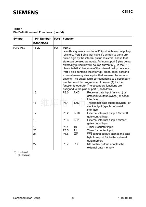
鈥?/div>
8 multiplexed input channels (port 6), which can also be used as digital inputs
10-bit resolution
Single or continuous conversion mode
Internal or external start-of-conversion trigger capability
Interrupt request generation after each conversion
Using successive approximation conversion technique via a capacitor array
Built-in hidden calibration of offset and linearity errors
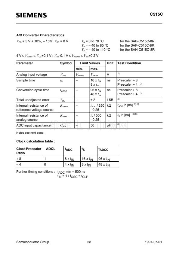
The main functional blocks of the A/D converter are shown in
figure 19.
The A/D converter uses basically two clock signals for operation : the input clock f
IN
(=1/t
IN
) and the
conversion clock f
ADC
(=1/t
ADC
). These clock signals are derived from the C515C system clock
f
OSC
which is applied at the XTAL pins. The input clock f
IN
is equal to f
OSC
. The conversion clock
is limited to a maximum frequency of 2 MHz and therefore must be adapted to f
OSC
by
programming the conversion clock prescaler. The table in
figure 18
shows the prescaler ratios and
the resulting A/D conversion times which must be selected for typical system clock rates.
MCU System Clock ADCL
Rate (f
OSC
)
2 MHz
4 MHz
6 MHz
8 MHz
10 MHz
Figure 18
A/D Converter Clock Selection
0
0
0
0
1
Conversion Clock
f
ADC
[MHz]
.5
1
1.5
2
1.25
Semiconductor Group
43
1997-07-01


 1
1
 2
2
 3
3
 4
4
 5
5
 6
6
 7
7
 8
8
 9
9
 10
10
 11
11
 12
12
 13
13
 14
14
 15
15
 16
16
 17
17
 18
18
 19
19
 20
20
 21
21
 22
22
 23
23
 24
24
 25
25
 26
26
 27
27
 28
28
 29
29
 30
30
 31
31
 32
32
 33
33
 34
34
 35
35
 36
36
 37
37
 38
38
 39
39
 40
40
 41
41
 42
42
 43
43
 44
44
 45
45
 46
46
 47
47
 48
48
 49
49
 50
50
 51
51
 52
52
 53
53
 54
54
 55
55
 56
56
 57
57
 58
58
 59
59
 60
60
 61
61
 62
62
 63
63
 64
64
 65
65
 66
66
 67
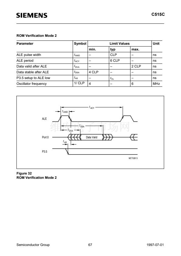
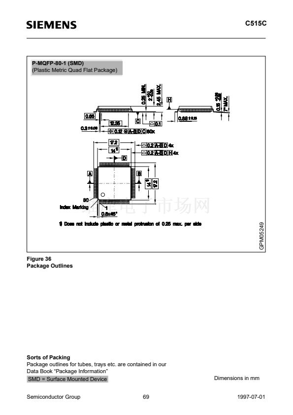
67
 68
68
 69
69
