鈭?/div>
Metal film resistor 鹵1%
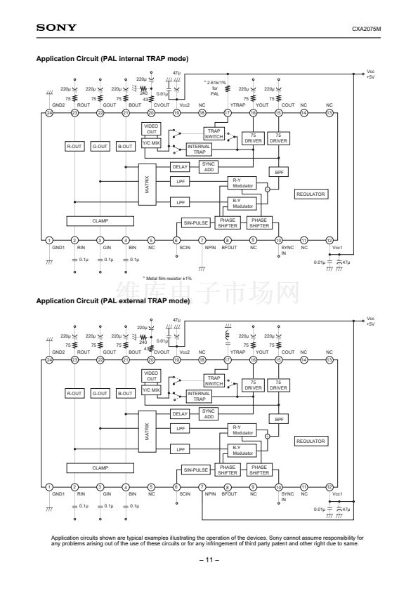
Application Circuit (PAL external TRAP mode)
47碌
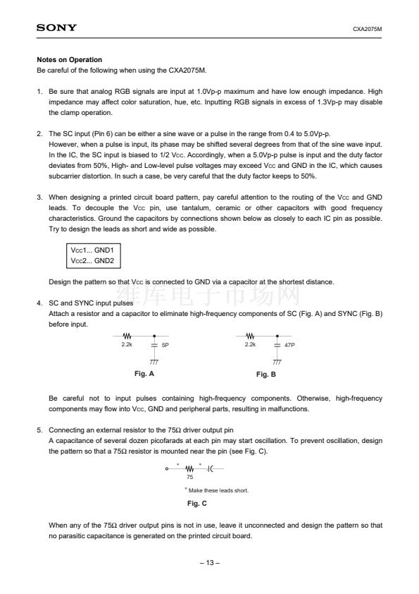
220碌
220碌
75
GND2
24
23
ROUT
22
220碌
75
GOUT
21
220碌
75
240
BOUT
43
20
VIDEO
OUT
R-OUT
G-OUT
B-OUT
Y/C MIX
0.01碌
CVOUT
19
Vcc2
NC
18
17
75
YTRAP
16
75
YOUT
15
COUT
NC
14
NC
13
220碌
220碌
Vcc
+5V
TRAP
SWITCH
INTERNAL
TRAP
DELAY
SYNC
ADD
75
DRIVER
75
DRIVER
BPF
R-Y
Modulator
REGULATOR
B-Y
Modulator
PHASE
SHIFTER
8
PHASE
SHIFTER
9
NC
10
SYNC
IN
11
NC
0.01碌
12
Vcc1
47碌
MATRIX
LPF
LPF
CLAMP
SIN-PULSE
1
GND1
2
RIN
0.1碌
3
GIN
0.1碌
4
BIN
0.1碌
5
NC
6
SCIN
7
NPIN
BFOUT
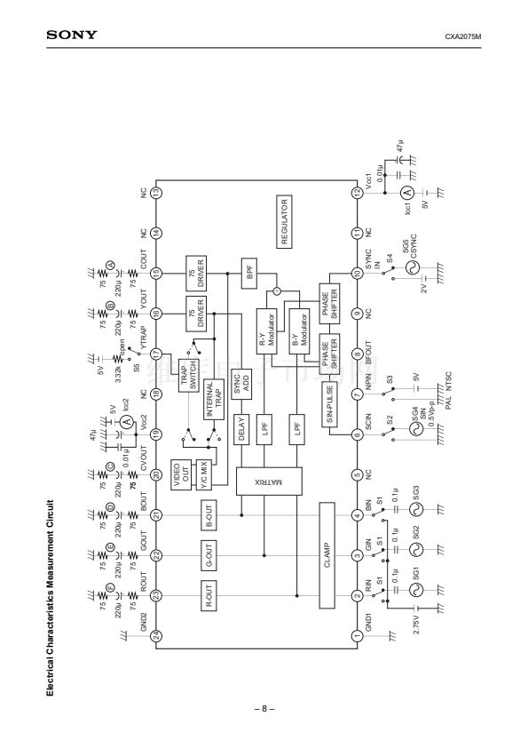
Application circuits shown are typical examples illustrating the operation of the devices. Sony cannot assume responsibility for
any problems arising out of the use of these circuits or for any infringement of third party patent and other right due to same.
鈥?11 鈥?/div>
prev
next


 1
1
 2
2
 3
3
 4
4
 5
5
 6
6
 7
7
 8
8
 9
9
 10
10
 11
11
 12
12
 13
13
 14
14
 15
15
