FEDL7540-03
隆 Semiconductor
MSM7540/7560
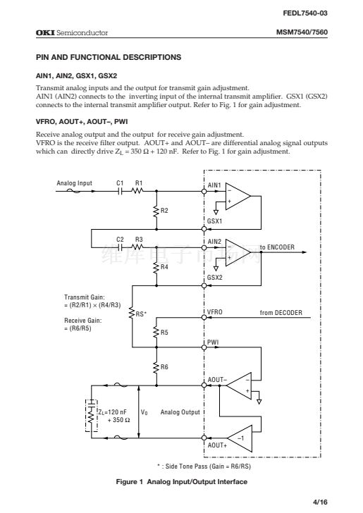
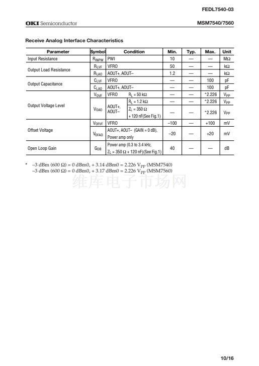
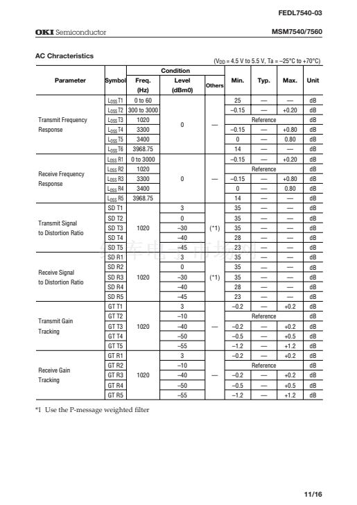
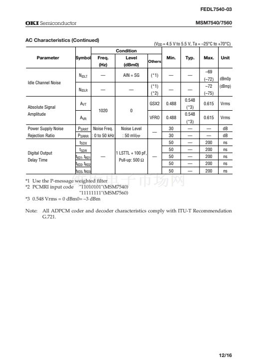
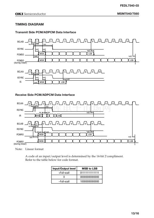
PIN AND FUNCTIONAL DESCRIPTIONS
AIN1, AIN2, GSX1, GSX2
Transmit analog inputs and the output for transmit gain adjustment.
AIN1 (AIN2) connects to the inverting input of the internal transmit amplifier. GSX1 (GSX2)
connects to the internal transmit amplifier output. Refer to Fig. 1 for gain adjustment.
VFRO, AOUT+, AOUT鈥? PWI
Receive analog output and the output for receive gain adjustment.
VFRO is the receive filter output. AOUT+ and AOUT鈥?are differential analog signal outputs
which can directly drive Z
L
= 350
W
+ 120 nF. Refer to Fig. 1 for gain adjustment.
Analog Input
C1
R1
AIN1
鈥?/div>
+
R2
GSX1
C2
R3
AIN2
鈥?/div>
+
to ENCODER
R4
GSX2
Transmit Gain:
= (R2/R1)
樓
(R4/R3)
RS*
Receive Gain:
= (R6/R5)
R5
PWI
VFRO
from DECODER
R6
AOUT鈥?/div>
鈥?/div>
+
Z
L
=120 nF
+ 350
W
V
0
Analog Output
鈥?
AOUT+
* : Side Tone Pass (Gain = R6/RS)
Figure 1 Analog Input/Output Interface
4/16


 1
1
 2
2
 3
3
 4
4
 5
5
 6
6
 7
7
 8
8
 9
9
 10
10
 11
11
 12
12
 13
13
 14
14
 15
15
 16
16
