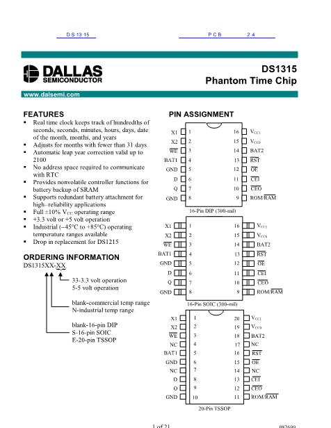
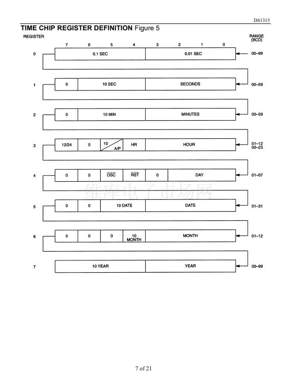
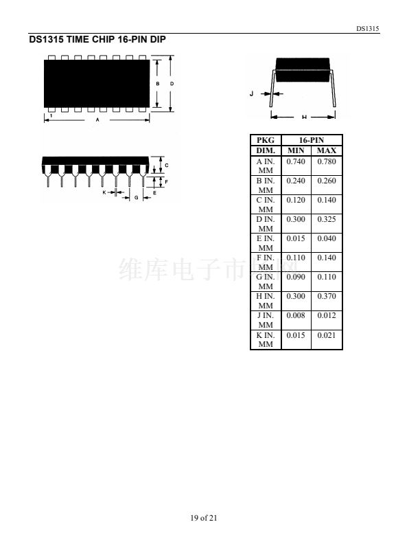
DS1315
NOTES:
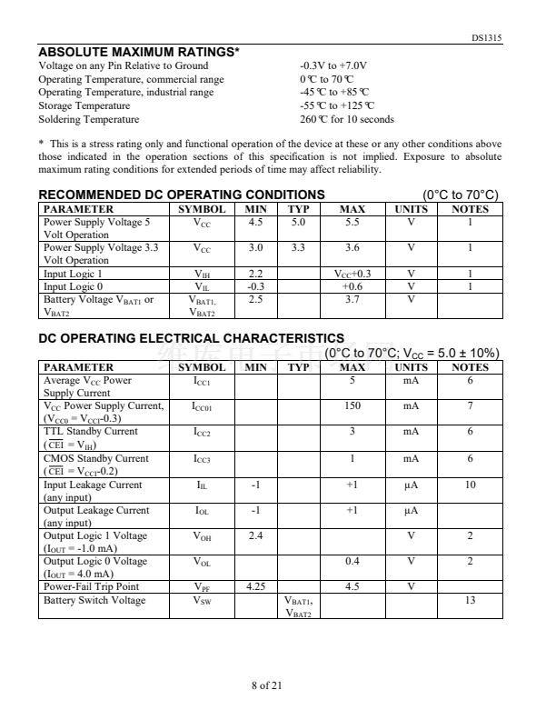
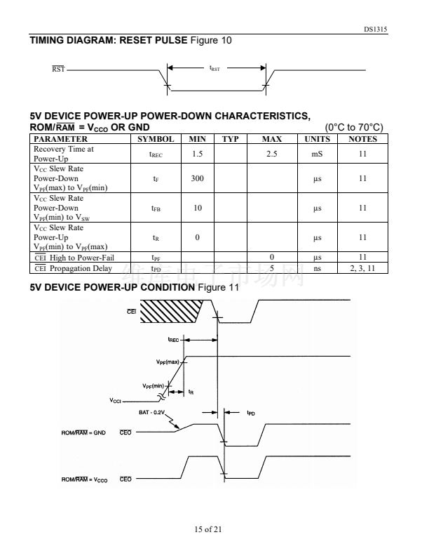
1. All voltages are referenced to ground.
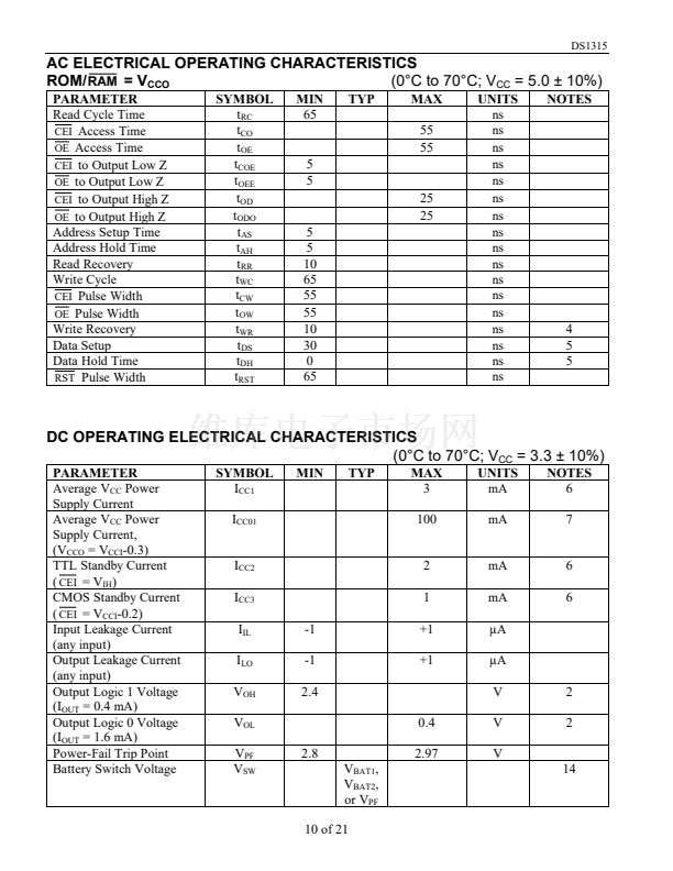
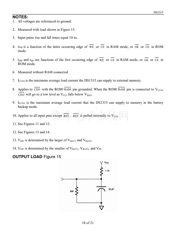
2. Measured with load shown in Figure 15.
3. Input pulse rise and fall times equal 10 ns.
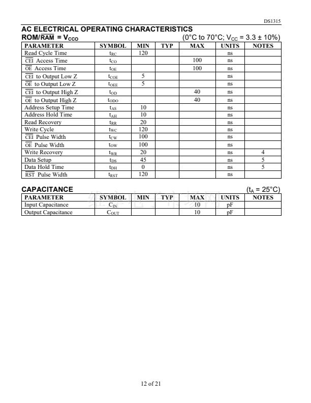
4. t
WR
is a function of the latter occurring edge of
WE
or
CE
in RAM mode, or
OE
or
CE
in ROM
mode.
5. t
DH
and t
DS
are functions of the first occurring edge of
WE
or
CE
in RAM mode, or
OE
or
CE
in
ROM mode.
6. Measured without RAM connected.
7. I
CCO1
is the maximum average load current the DS1315 can supply to external memory.
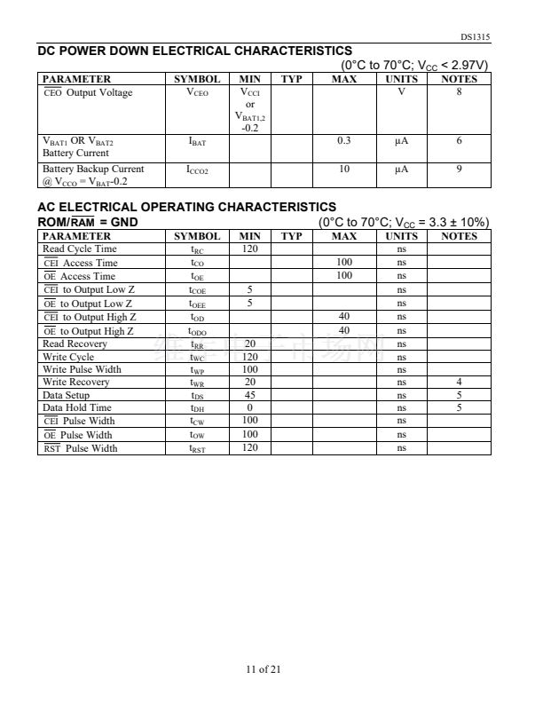
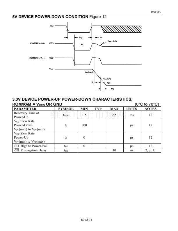
8. Applies to
CEO
with the ROM/
RAM
pin grounded. When the ROM/
RAM
pin is connected to V
CCO
,
CEO
will go to a low level as V
CCI
falls below V
BAT
.
9. I
CCO2
is the maximum average load current that the DS1315 can supply to memory in the battery
backup mode.
10. Applies to all input pins except
RST
.
RST
is pulled internally to V
CCI
.
11. See Figures 11 and 12.
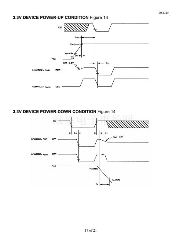
12. See Figures 13 and 14.
13. V
SW
is determined by the larger of V
BAT1
and V
BAT2
.
14. V
SW
is determined by the smaller of V
BAT1
, V
BAT2
, and V
PF
.
OUTPUT LOAD
Figure 15
18 of 21


 1
1
 2
2
 3
3
 4
4
 5
5
 6
6
 7
7
 8
8
 9
9
 10
10
 11
11
 12
12
 13
13
 14
14
 15
15
 16
16
 17
17
 18
18
 19
19
 20
20
 21
21
