鈥?/div>
Frequency range 75 ~ 180MHz.
Internal phase locked loop will allow spread spec-
trum modulation on reference clock to pass to the
outputs (up to 100kHz SST modulation).
Zero input - output delay.
Less than 700 ps device - device skew.
Less than 250 ps skew between outputs.
Less than 150 ps cycle - cycle jitter.
Output Enable function tri-state outputs.
3.3V operation.
Available in 8-Pin 150mil SOIC
GREEN
package.
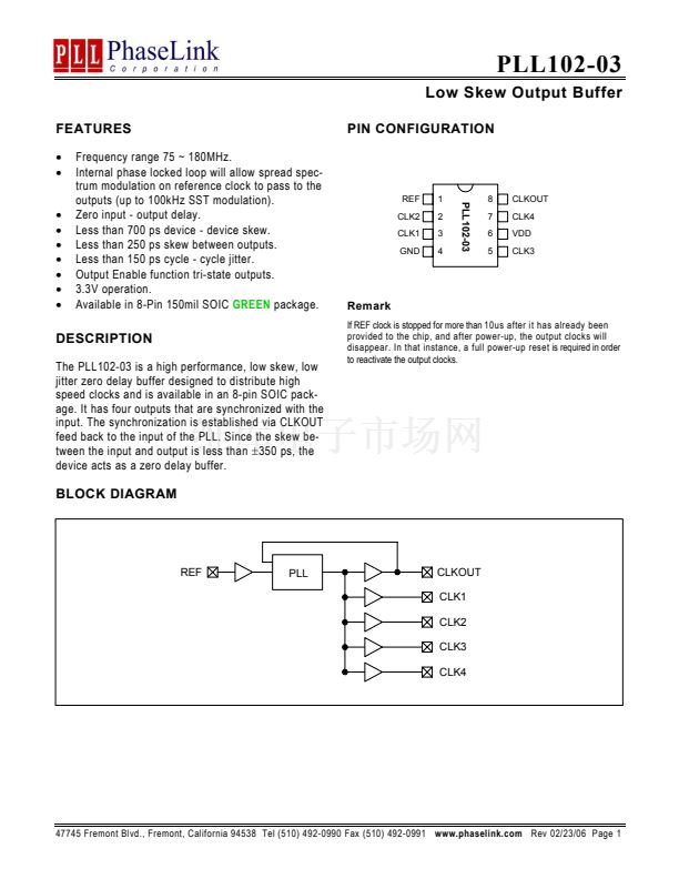
PIN CONFIGURATION
REF
CLK2
CLK1
GND
1
2
3
4
8
7
6
5
CLKOUT
CLK4
VDD
CLK3
PLL102-03
Remark
If REF clock is stopped for more than 10us after it has already been
provided to the chip, and after power-up, the output clocks will
disappear. In that instance, a full power-up reset is required in order
to reactivate the output clocks.
DESCRIPTION
The PLL102-03 is a high performance, low skew, low
jitter zero delay buffer designed to distribute high
speed clocks and is available in an 8-pin SOIC pack-
age. It has four outputs that are synchronized with the
input. The synchronization is established via CLKOUT
feed back to the input of the PLL. Since the skew be-
tween the input and output is less than
鹵350
ps, the
device acts as a zero delay buffer.
BLOCK DIAGRAM
REF
PLL
CLKOUT
CLK1
CLK2
CLK3
CLK4
47745 Fremont Blvd., Fremont, California 94538 Tel (510) 492-0990 Fax (510) 492-0991
www.phaselink.com
Rev 02/23/06 Page 1


 1
1
 2
2
 3
3
 4
4
 5
5
 6
6
