M54/74HC374
M54/74HC534
OCTAL D-TYPE FLIP FLOP WITH 3 STATE OUTPUT
HC374 NON INVERTING - HC534 INVERTING
.
.
.
.
.
.
.
.
HIGH SPEED
f
MAX
= 77 MHz (TYP.) AT V
CC
= 5 V
LOW POWER DISSIPATION
I
CC
= 4
碌A(chǔ)
(MAX.) AT T
A
= 25
擄C
HIGH NOISE IMMUNITY
V
NIH
= V
NIL
= 28 % V
CC
(MIN)
OUTPUT DRIVE CAPABILITY
15 LSTTL LOADS
SYMMETRICAL OUTPUT IMPEDANCE
I
OL
=
錚
OH
錚?
6 mA (MIN.)
BALANCED PROPAGATION DELAYS
t
PLH
= t
PHL
WIDE OPERATING VOLTAGE RANGE
V
CC
(OPR) = 2 V TO 6 V
PIN AND FUNCTION COMPATIBLE
WITH 54/74LS374/534
B1R
(Plastic Package)
F1R
(Ceramic Package)
M1R
(Micro Package)
C1R
(Chip Carrier)
ORDER CODES :
M54HCXXXF1R
M74HCXXXM1R
M74HCXXXB1R
M74HCXXXC1R
DESCRIPTION
The M54/74HC374, M54/74HC534, are high speed
CMOS OCTAL D-TYPE FLIP FLOP WITH 3-STATE
OUTPUTS fabricated with in silicon gate C
2
MOS
technology. They have the same high speed per-
formance of LSTTL combined with true CMOS low
power comsuption. These8-bit D-type flip-flops are
controlled by a clock input (CK) and an ouput enable
input (OE). On the positive transition of the clock, the
Q outputs will be set to the logic state that were setup
at the D inputs (HC374) or their complements
(HC534).
While the OE input is low, the eight outputs will be
in a normal logic state (high or low logic level), and
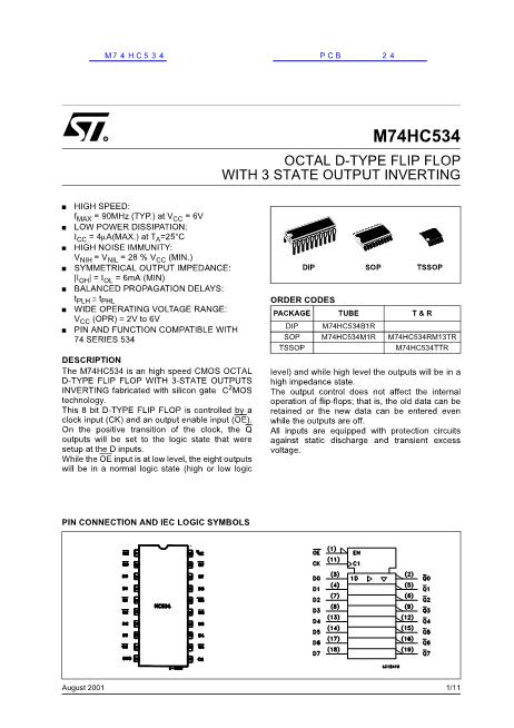
PIN CONNECTION
(top view)
while high level, the outputs will be in a high imped-
ance state. The output control does not affect the in-
ternal operation of flip-flops. That is, the old data can
be retained or the new data can be entered even
while the outputs are off. The application engineer
has a choice of combination of inverting and non-in-
verting outputs. The HC374 and HC574 are identi-
cal, apart from pin layout. The 3-state output
configuration and the wide choice of outline make
bus-organized systems simple. All inputs are
equipped with protection circuits against static dis-
charge and transient excess voltage.
March 1993
1/13


 1
1
 2
2
 3
3
 4
4
 5
5
 6
6
 7
7
 8
8
 9
9
 10
10
 11
11
 12
12
 13
13
