Integrated
Circuit
Systems, Inc.
Preliminary Information
M1040
VCSO B
ASED
C
LOCK
PLL
WITH
A
UTO
S
WITCH
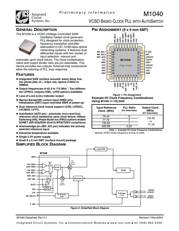
P
IN
A
SSIGNMENT
(9 x 9 mm SMT)
MR_SEL2
GND
AUTO
DIF_REF0
nDIF_REF0
REF_SEL
DIF_REF1
nDIF_REF1
VCC
MR_SEL1
MR_SEL0
REF_ACK
LOL
NBW
VCC
DNC
DNC
DNC
27
26
25
24
23
22
21
20
19
G
ENERAL
D
ESCRIPTION
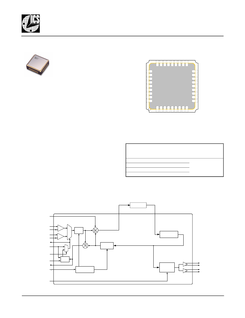
The M1040 is a VCSO (Voltage Controlled SAW
Oscillator) based clock generator
PLL designed for clock protection,
frequency translation and jitter
attenuation in OC-12/48 class optical
networking systems. It features dual
differential inputs with two modes of
input selection: manual and
automatic upon clock failure. The clock multiplication
ratios and output divider ratio are pin selectable. This
device provides two outputs. External loop components
allow the tailoring of PLL loop response.
F
EATURES
鈼?/div>
Integrated SAW (surface acoustic wave) delay line;
low phase jitter of < 0.5ps rms, typical (12kHz to
20MHz)
鈼?/div>
Output frequencies of 62.5 to 175 MHz
*
; Two differen-
tial LVPECL outputs (CML, LVDS options available)
鈼?/div>
Loss of Lock (LOL) indicator output
鈼?/div>
Narrow Bandwidth control input (NBW pin);
Initialization (INIT) input overrides NBW at power-up
鈼?/div>
Dual reference clock inputs support LVDS, LVPECL,
LVCMOS, LVTTL
鈼?/div>
AutoSwitch (AUTO pin) - automatic (non-revertive)
reference clock reselection upon clock failure; Hitless
Switching (HS), Phase Build-out (PBO) options enable
SONET (GR-253)/SDH (G.813) MTIE/TDEV compliance
鈼?/div>
Acknowledge pin (REF_ACK pin) indicates the actively
selected reference input
鈼?/div>
Industrial temperature available
鈼?/div>
Single 3.3V power supply
鈼?/div>
Small 9 x 9 mm SMT (surface mount) package
28
29
30
31
32
33
34
35
36
M1040
(Top View)
18
17
16
15
14
13
12
11
10
P_SEL
INIT
nFOUT0
FOUT0
GND
nFOUT1
FOUT1
VCC
GND
Figure 1: Pin Assignment
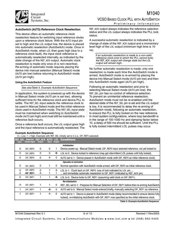
Example I/O Clock Frequency Combinations
Using
M1040-11-155.5200
Input Reference
Clock (MHz)
19.44
77.76
155.52
622.08
PLL Ratio
(Pin Selectable)
GND
GND
GND
OP_IN
nOP_OUT
nVC
VC
OP_OUT
nOP_IN
1
2
3
4
5
6
7
8
9
Output Clock
(MHz)
(Pin Selectable)
8
2
1
0.25
155.52
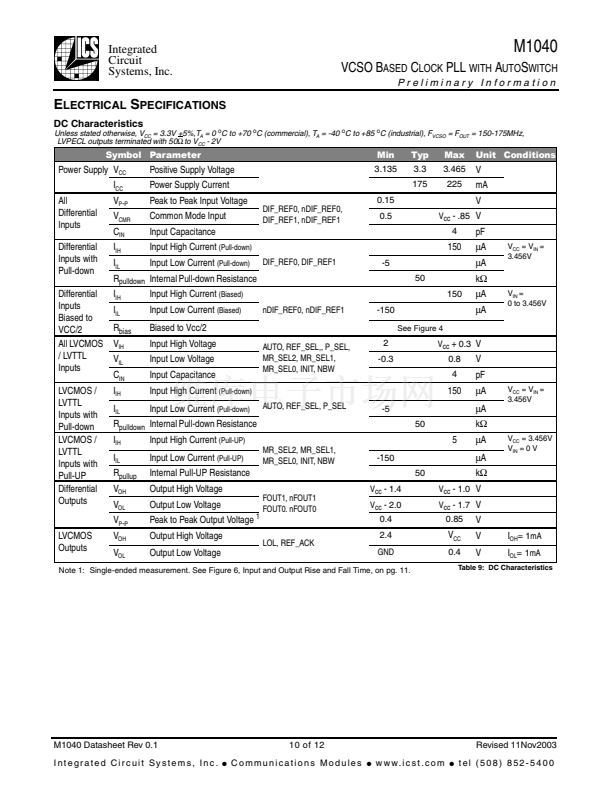
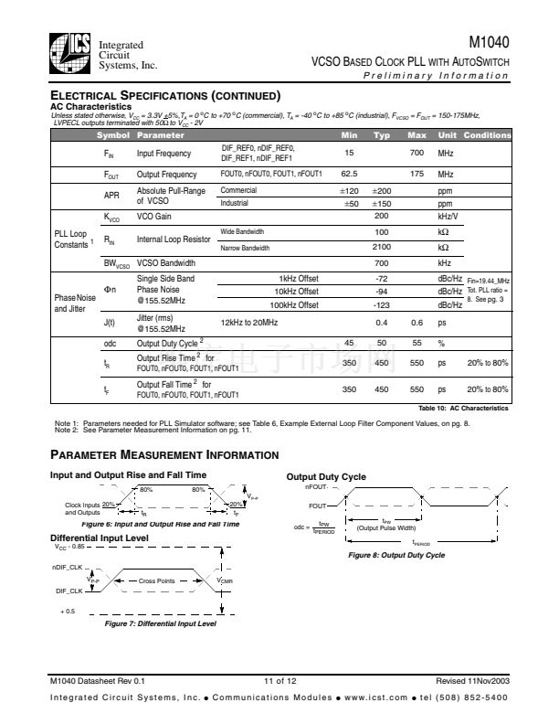
or
77.76
Table 1: Example I/O Clock Frequency Combinations
* Specify VCSO center frequency at time of order.
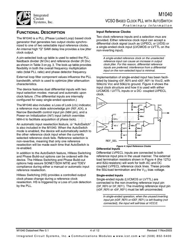
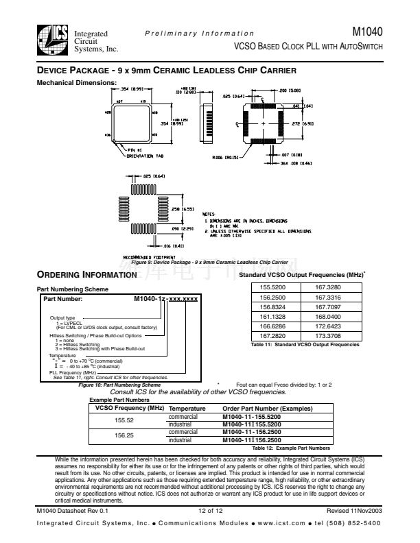
S
IMPLIFIED
B
LOCK
D
IAGRAM
Loop Filter
M1040
NBW
MUX
PLL
Phase
Detector
DIF_REF0
nDIF_REF0
DIF_REF1
nDIF_REF1
REF_ACK
REF_SEL
AUTO
Auto
INIT
LOL
MR_SEL2:0
3
Ref Sel
0
R Div
VCSO
1
0
1
M Divider
LOL
Phase
Detector
M / R Divider
P Divider
(1 or 2)
FOUT0
nFOUT0
FOUT1
nFOUT1
LUT
P_SEL
Figure 2: Simplified Block Diagram
M1040 Datasheet Rev 0.1
M1040 VCSO Based Clock PLL with AutoSwitch
Revised 11Nov2003
鈼?/div>
Integrated Circuit Systems, Inc.
Communications Modules
鈼?/div>
w w w. i c s t . c o m
鈼?/div>
tel (508) 852-5400
M1040-11I155.5200相關(guān)型號PDF文件下載
-
型號
版本
描述
廠商
下載
-
英文版
VCSO BASED CLOCK PLL WITH AUTOSWITCH
ICS
-
英文版
VCSO BASED CLOCK PLL WITH AUTOSWITCH
ICST [Inte...
-
英文版
VCSO BASED CLOCK PLL WITH AUTOSWITCH
ICS
-
英文版
VCSO BASED CLOCK PLL WITH AUTOSWITCH
ICST [Inte...
-
英文版
VCSO BASED CLOCK PLL WITH AUTOSWITCH
ICS
-
英文版
VCSO BASED CLOCK PLL WITH AUTOSWITCH
ICST [Inte...
-
英文版
VCSO BASED CLOCK PLL WITH AUTOSWITCH
ICS
-
英文版
VCSO BASED CLOCK PLL WITH AUTOSWITCH
ICST [Inte...
-
英文版
VCSO BASED CLOCK PLL WITH AUTOSWITCH
ICS
-
英文版
VCSO BASED CLOCK PLL WITH AUTOSWITCH
ICST [Inte...


 1
1
 2
2
 3
3
 4
4
 5
5
 6
6
 7
7
 8
8
 9
9
 10
10
 11
11
 12
12
